Liquid crystal display device and method for producing the same

a liquid crystal display and liquid crystal technology, applied in the field of liquid crystal display devices, can solve the problems of ultraviolet radiation degradation of liquid crystal materials, easy damage to liquid crystal materials, etc., and achieve the effects of promoting polymerization, high display quality, and promoting polymerization

Inactive Publication Date: 2011-12-29
SHARP KK
View PDF4 Cites 4 Cited by
  • Summary
  • Abstract
  • Description
  • Claims
  • Application Information

AI Technical Summary

Benefits of technology

[0019]A liquid crystal display device of the present invention is a reflective liquid crystal display device including: substrates wherein electrodes formed on one of the substrates are paired with electrodes formed on the other one of the substrates; a liquid crystal sandwiched between the substrates, the liquid crystal being arranged by dispersing liquid crystal drops in a polymer film or by forming a polymer network in a liquid crystal layer; and an ultraviolet-absorbing layer provided between at least one of the substrates and the pair of electrodes, the ultraviolet-absorbing layer having a transmittance ratio (T (365 nm) / T (315 nm)) of not less than 6.3 where a transmittance at a wavelength of 365 nm is (T (365 nm)) and a transmittance at a wavelength of 315 nm is (T (315 nm)).
[0020]With the above arrangement, ultraviolet having a wavelength of 365 nm necessary for polymerization is hardly absorbed by the ultraviolet-absorbing layer, thereby sufficiently promoting a polymerization reaction for preparing a polymer. As a result, it is possible to sufficiently restrain that the liquid crystal is deteriorated by ultraviolet, thereby resulting in that a liquid crystal display device having a high display quality can be produced.
[0021]A reflective liquid crystal display device of the present invention, including: a first insulating substrate on which (i) a memory including a plurality of active elements, (ii) an interlayer insulating film and (iii) a reflective electrode are formed in this order; a second insulating substrate on which a transparent electrode is formed, the first insulating substrate and the second insulating substrate being attached to each other such that the reflective electrode formed on the first insulating substrate faces the transparent electrode formed on the second insulating substrate; a liquid crystal sandwiched between the first insulating substrate and the second insulating substrate, the liquid crystal being arranged by dispersing liquid crystal drops in a polymer film or by forming a polymer network in a liquid crystal layer; and an ultraviolet-absorbing layer provided between the second insulating substrate and the transparent electrode, the ultraviolet-absorbing layer having a transmittance ratio (T (365 nm) / T (315 nm)) of not less than 6.3 where (T (365 nm)) is a transmittance at a wavelength of 365 nm and T (315 nm) is a transmittance at a wavelength of 315 nm.
[0022]With the above arrangement, ultraviolet having a wavelength of 365 nm necessary for polymerization for preparing a polymer is hardly absorbed by the ultraviolet-absorbing layer, thereby sufficiently promoting the polymerization. On the other hand, ultraviolet having a wavelength of 315 nm is sufficiently blocked, thereby making it possible to restrain that a liquid crystal material is deteriorated by the ultraviolet having a wavelength of 315 nm which is emitted from a fluorescent lamp or an exposure device used in a production process and which cannot be removed by an ultraviolet cut filter. This arrangement can restrain a reduction in reflectance, thereby making it possible to produce a reflective liquid crystal display device which can perform high-quality display with high contrast and less flickers.
[0023]A method for producing a reflective liquid crystal display device of the present invention including the steps of: preparing a first insulating substrate on which (i) a memory including a plurality of active elements, (ii) an interlayer insulating film and (iii) a reflective electrode are formed in this order; preparing a second insulating substrate on which an ultraviolet-absorbing layer and a transparent electrode are formed in this order, the ultraviolet-absorbing layer having a transmittance ratio (T (365 nm) / T (315 nm)) of not less than 6.3 where (T (365 nm)) is a transmittance at a wavelength of 365 nm and (T (315 nm)) is a transmittance at a wavelength of 315 nm; attaching the first insulating substrate and the second substrate to each other such that the reflective electrode formed on the first insulating substrate faces the transparent electrode formed on the second insulating substrate; providing a liquid crystal, a monomer and a photopolymerization initiator between the first insulating substrate and the second insulating substrate; and polymerizing the monomer by irradiating the reflective liquid crystal display device from the second insulating substrate with ultraviolet, the ultraviolet having an intensity of not less than 30 mW / cm2 at a wavelength of 365 nm at a liquid crystal panel surface.
[0024]According to the above method, ultraviolet having a wavelength of 365 nm necessary to initiate polymerization for preparing a polymer is hardly absorbed by the ultraviolet-absorbing layer, and further, the polymerization is sufficiently promoted because an intensity of irradiation on the liquid crystal panel surface is 30 mW / cm2 or more. Further, ultraviolet having a wavelength of 315 nm is sufficiently blocked, thereby making it possible to restrain that a liquid crystal material is deteriorated by the ultraviolet having a wavelength of 315 nm which is emitted from a fluorescent lamp or an exposure device used in a production process and which cannot be removed by an ultraviolet cut filter. This can restrain a reduction in reflectance, thereby making it possible to produce a reflective liquid crystal display device which can perform high-quality display with high contrast and less flickers. Further, in the above method, it is possible to perform, under light emitted from the fluorescent lamp, various processes, such as cutting of a glass after a display element is formed, etching of the glass to reduce the display element in its thickness, and attaching of an optical film to the display element. Accordingly, it is possible to perform these processes more flexibly.

Problems solved by technology

However, it is known that liquid crystal materials are degraded by ultraviolet radiation, and ionic impurities caused by the degradation deteriorate properties of the liquid crystal materials.
Especially, it is well known that liquid crystals used in the PDLC method and the PNLC method are easily affected by ultraviolet light.
As a result, an effective voltage applied to the liquid crystal layer is reduced, thereby causing flickers.

Method used


Image

  • Liquid crystal display device and method for producing the same
  • Liquid crystal display device and method for producing the same
  • Liquid crystal display device and method for producing the same

Examples


examples

[0047]The following describes in detail the present invention on the basis of Examples.

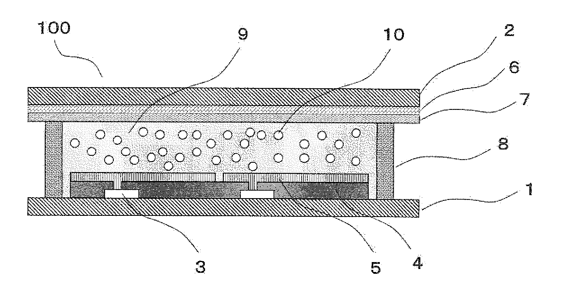
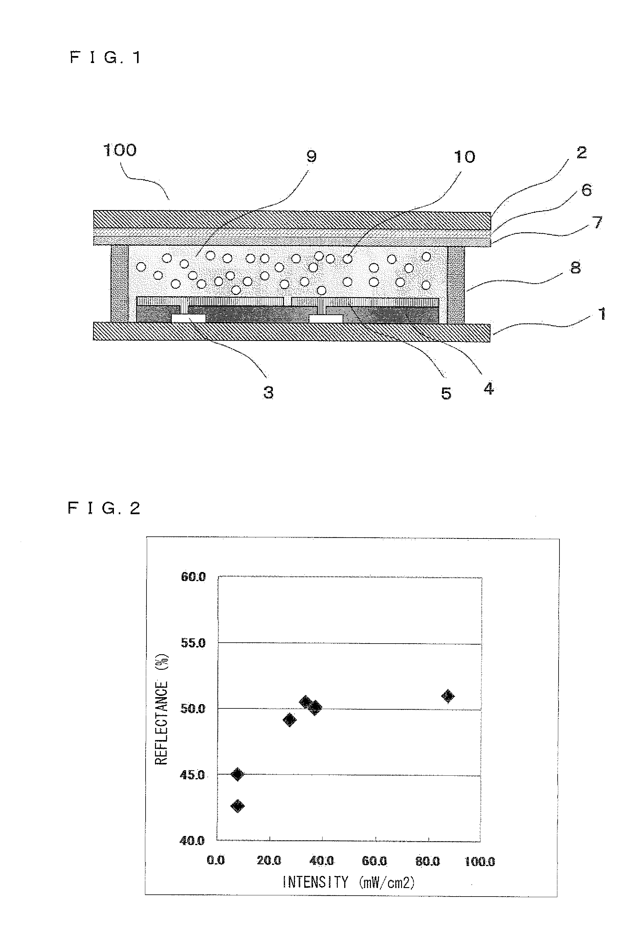
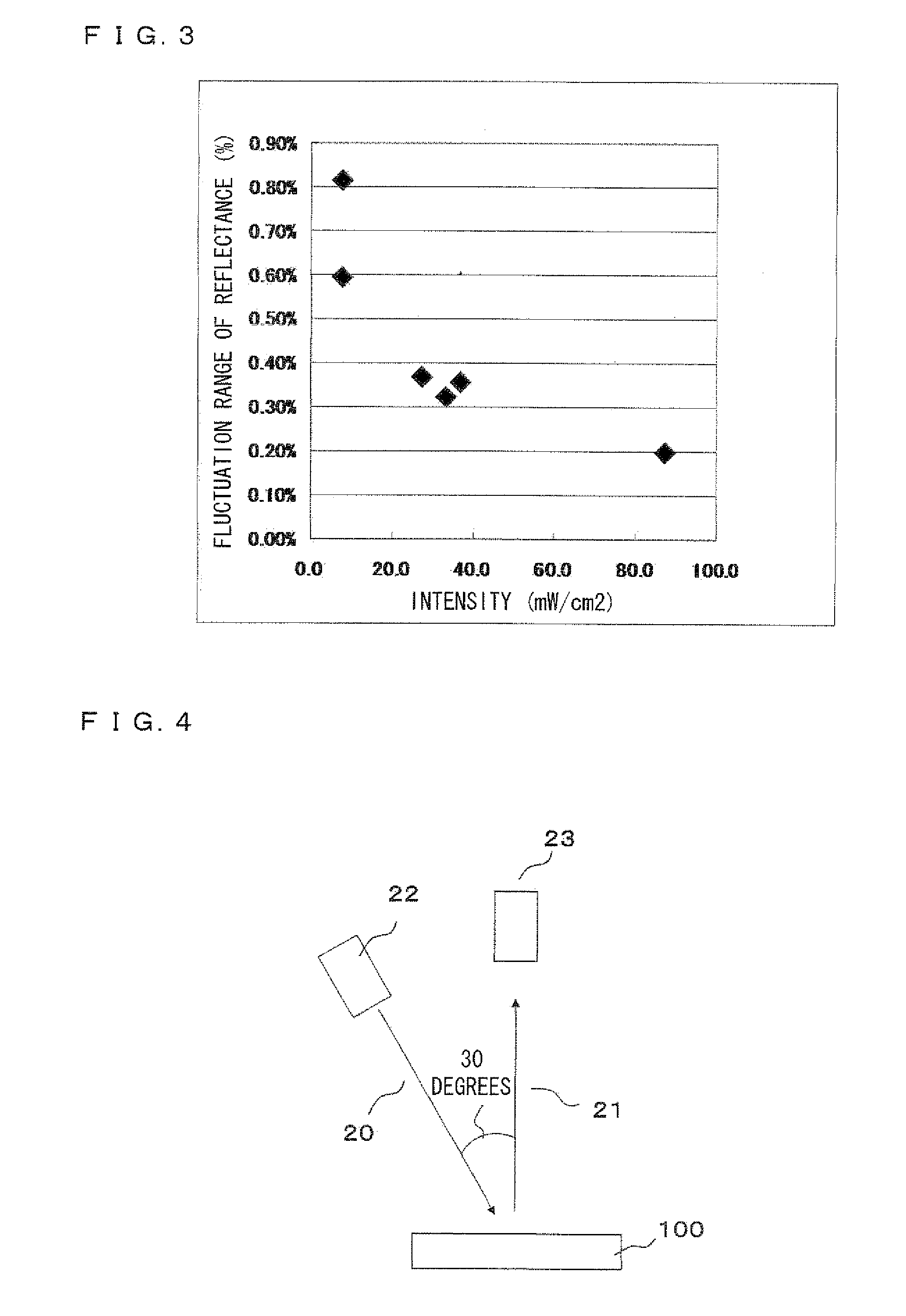
[0048]A glass substrate having a thickness of 0.7 mm was used for a first insulating substrate. FIG. 5 illustrates a plain view of a pixel circuit used in the present example. VLAs (pixel voltage supply lines having a phase identical to that of a common electrode) 31 formed parallel to a longitudinal direction or a lateral direction of the pixel circuit surround a region. The region corresponds to a subpixel. The subpixel includes twelve TFT elements 3 constituting two static RAMs. The TFT elements 3 and wirings are provided over the subpixel of the present example. A Vdd 33 and a Vss 34 are wirings for supplying a voltage to the static RAMs. A GL 35 and a GLS 36 are wirings for a ground electric potential. An SL 37 is a wiring for supplying an image signal. A reflective electrode is electrically connected to the VLAs 31 or a VLB (pixel voltage supply line having a phase opposite to that of the co...


PUM

PropertyMeasurementUnit
thicknessaaaaaaaaaa
wavelengthaaaaaaaaaa

Abstract

An ultraviolet-absorbing layer is provided between an insulating substrate and a transparent electrode, the ultraviolet-absorbing layer having a transmittance ratio (T (365 nm) / T (315 nm)) of not less than 6.3 where (T (365 nm)) is a transmittance at a wavelength of 365 nm and (T (315 nm)) is a transmittance at a wavelength of 315 nm.

Description

TECHNICAL FIELD[0001]The present invention relates to a liquid crystal display device and a method for producing the liquid crystal display device.BACKGROUND ART[0002]Recently, reflective display devices using light of ambient environments are highly expected especially as display devices of mobile phones, electronic books, and the like. This is because the reflective display devices do not need a backlight and they have such advantages that they are reduced in power consumption, thickness, and weight.[0003]Among these reflective display devices, reflective LCD devices are being widely used. Some of the reflective LCD devices employ a method in which an excellent black display is attained by use of a polarizing plate and a liquid crystal layer that controls a polarization state of light passing therethrough. Further, some of the reflective LCD devices employ a method in which an excellent white display is attained by use of a liquid crystal layer that controls a scattering state of ...

Claims


Application Information

Patent Timeline
Patent Type & Authority Applications(United States)
IPC IPC(8): G02F1/1335H05K13/00
CPCG02F1/1334Y10T29/49002G02F2201/086G02F1/133509
Inventor ASAOKA, YASUSHIMINOURA, KIYOSHISATOH, EIJIDEGUCHI, KAZUHIROFUJIWARA, SAYURIMIYAMOTO, KENJI
Owner SHARP KK
Why Eureka
Try Eureka