

Method of setting thickness of dielectric and substrate processing apparatus having dielectric disposed in electrode
a technology of substrate processing and dielectric, which is applied in the direction of fluid pressure measurement, instruments, vacuum gauges, etc., can solve the problems of fast consumption of dielectric formed in the upper electrod
- Summary
- Abstract
- Description
- Claims
- Application Information
AI Technical Summary
Benefits of technology
Problems solved by technology
Method used
Image

Examples
example
[0059]An embodiment of the present invention will be described as follows.
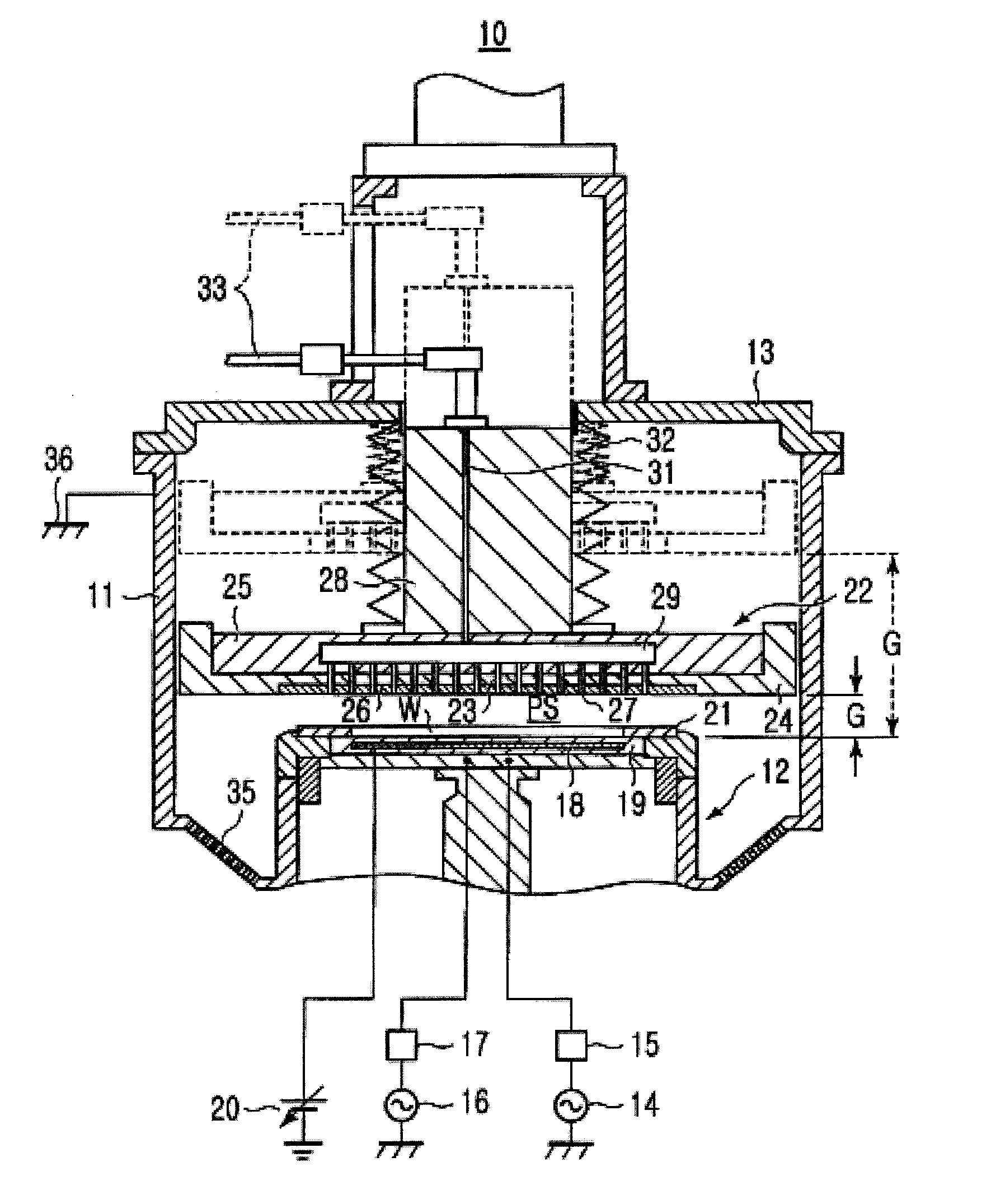
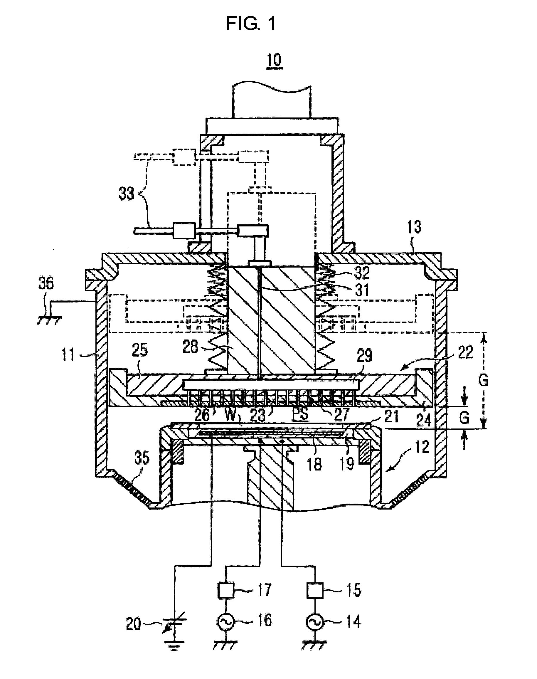
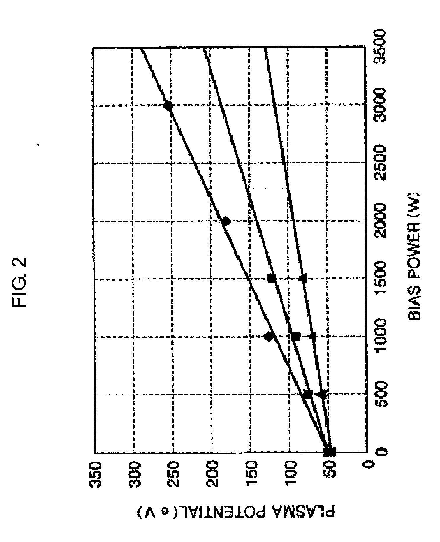
[0060]In the substrate processing apparatus 10, the thickness of the dielectric 26 was set to be 10 mm. After that, the wafer W was transferred to the chamber 11, and plasma processes including the dry etching process or an ashing process under the following three processing conditions were performed repeatedly on the wafer W for 90 hours.
[0061]First processing condition: a pressure in the chamber 11 was 60 mTorr (8.00 Pa), the plasma generating power value was 500 W, the bias power value was 500 W, a flow of CF4 was 140 sccm, and a continuous processing time was 20 seconds.
[0062]Second processing condition: a pressure in the chamber 11 was 30 mTorr, the plasma generating power value was 2700 W, the bias power value was 2000 W, a flow rate of a mixture gas was CHF3:Ar:O2=100:1000:30 sccm, and a continuous processing time was 50 seconds.
[0063]Third processing condition: a pressure in the chamber 11 was 40 mTorr...
PUM
| Property | Measurement | Unit |
|---|---|---|
| Energy | aaaaa | aaaaa |
| Thickness | aaaaa | aaaaa |
| Electric potential / voltage | aaaaa | aaaaa |
Abstract
Description
Claims
Application Information