Device and method to conduct an electrochemical reaction on a surface of a semi-conductor substrate

a technology of semi-conductor substrates and electrochemical reactions, which is applied in the direction of electrophoretic coatings, cell components, electrolytic organic material coatings, etc., can solve the problem of uniform reaction and achieve the effect of uniform electrochemical reaction

Active Publication Date: 2012-01-05
ALCHIMER SA
View PDF7 Cites 11 Cited by
  • Summary
  • Abstract
  • Description
  • Claims
  • Application Information

AI Technical Summary

Benefits of technology

[0064]The invention provides numerous advantages.
[0065]The device according to the first aspect of the invention permits uniform illumination of a surface of a semiconductor substrate notably via specific homogenization means, for the purpose of achieving a uniform electrochemical reaction. The device according to the first aspect of the invention also permits this uniform lighting whilst guaranteeing scarcely perturbed field lines between the semiconductor substrate and the counter-electrode.

Problems solved by technology

Said devices have disadvantages however:they do not permit uniform illumination of the surface of the substrate, the reaction is therefore not conducted uniformly;no known device allows the conducting of electrochemical reactions activated by illumination on a substrate surface of greater size than a disc 50 mm in diameter;no device permits uniform illumination of the semiconductor substrate without substantially perturbing the electric field lines in the electrolyte between the substrate and the counter-electrode.

Method used


Image

  • Device and method to conduct an electrochemical reaction on a surface of a semi-conductor substrate
  • Device and method to conduct an electrochemical reaction on a surface of a semi-conductor substrate
  • Device and method to conduct an electrochemical reaction on a surface of a semi-conductor substrate

Examples


example 1

Preparation of a Poly-4-Vinylpyridine (P4VP) Film on a Substrate of Planar Wafer Type 200 mm in P-Doped Silicon (Known Per Se) Illuminated at Between 3,000 lux and 3,500 lux.

Substrate:

[0241]The substrate S used in this example is a disc of P-doped silicon, 200 mm in diameter and with a thickness of 750 μm and resistivity of 50 Ω·cm.

Electrolyte:

[0242]The electrolyte E used in this example is an aqueous solution prepared by adding 195 ml of 4-vinylpyridine (4-VP; 1.83 mol) to 2.8 L of 1.5 M HCl, then adding to this mixture 4.95 g of 4-nitrobenzene diazonium tetrafluoroborate (DNO2; 2.10−2 mol) which forms the electrochemically active species.

[0243]Device:

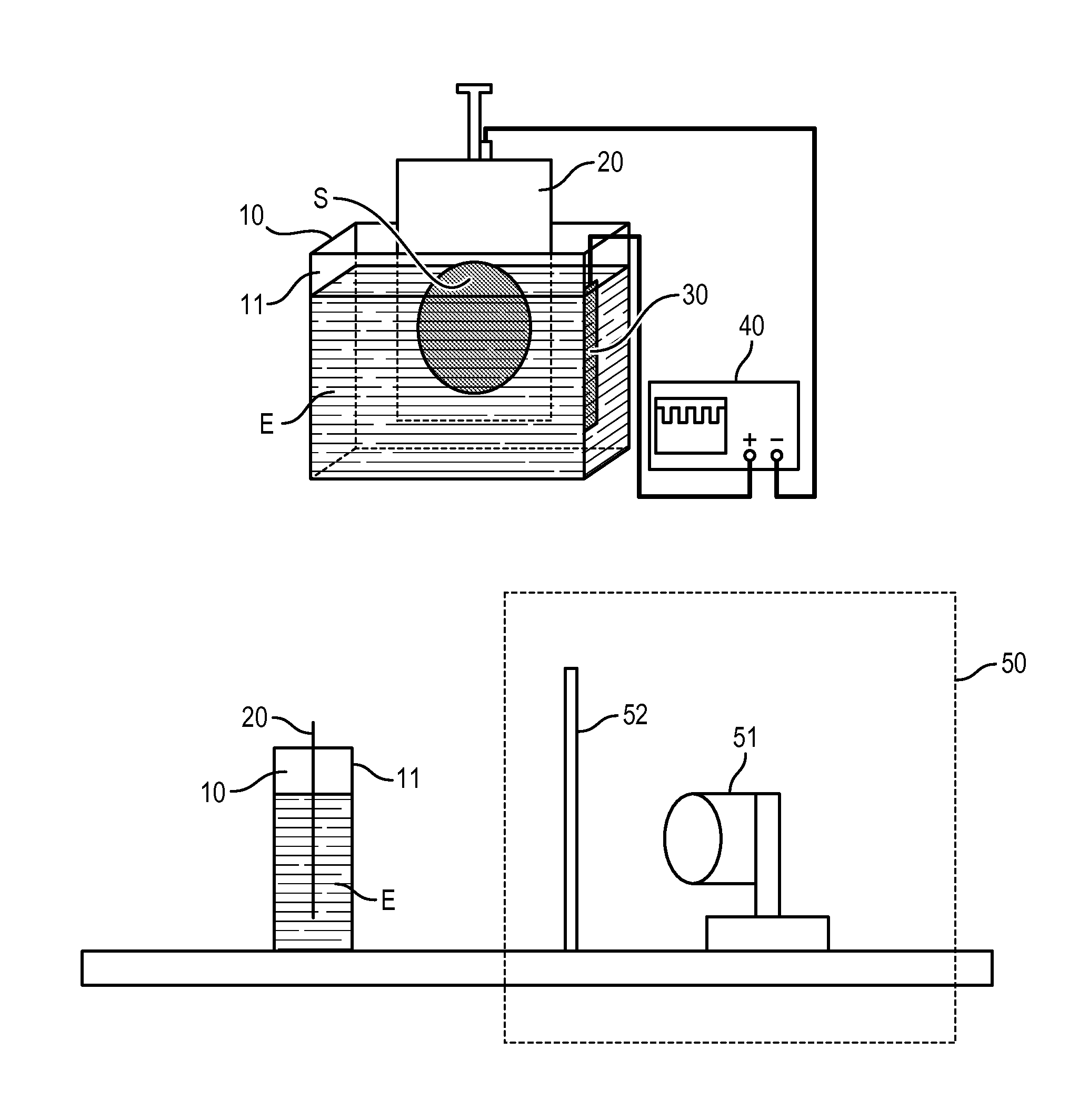
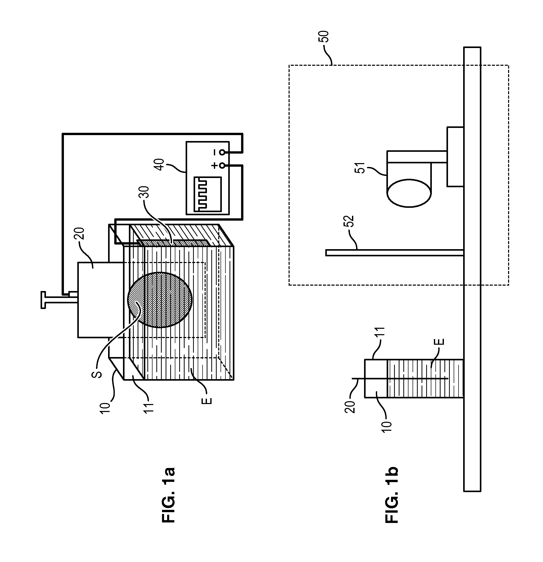
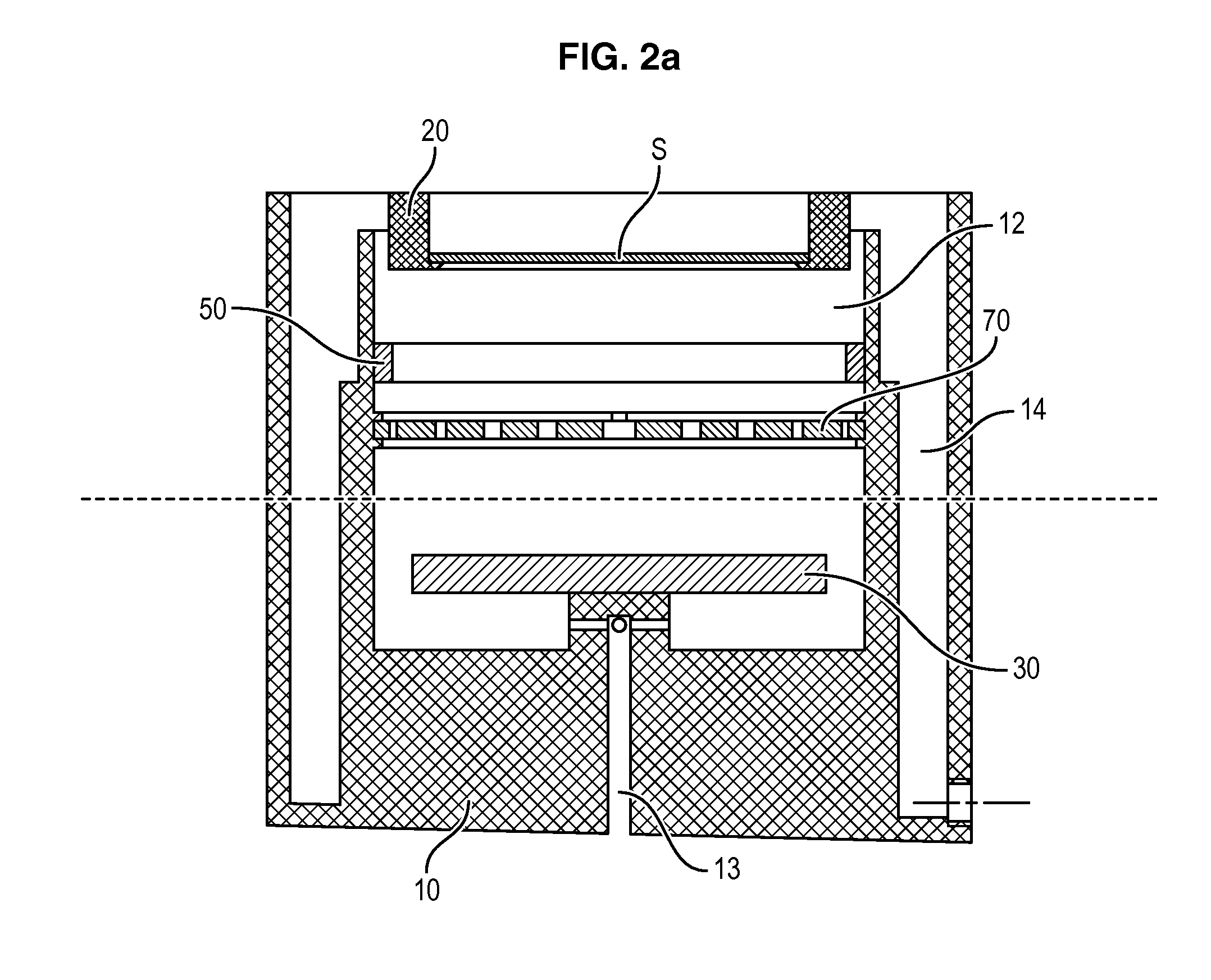
[0244]The device used to prepare the P4VP film is the device according to the first aspect of the invention illustrated in FIG. 1 in which:[0245]the container 10 is a parallelepiped tank of size 30 cm×30 cm×10 cm,[0246]the support 20 is in Teflon,[0247]the counter-electrode 30 is a rectangular anode in graphite of size 20 cm×5 cm×2 mm...

example 2

Preparation of a Poly-4-Vinylpyridine (P4VP) Film on a 200 mm Planar Wafer in P-Doped Silicon, Illuminated at Between 4,000 lux and 4,500 lux

Substrate:

[0268]The substrate S used is described in Example 1.

Electrolyte:

[0269]The electrolyte E used in this example is the one described in Example 1.

Device:

[0270]The device used to prepare the P4VP film is the device according to the first aspect of the invention illustrated in FIG. 1 in which:[0271]the container 10 is a parallelepiped tank of size 30 cm×30 cm×10 cm,[0272]the support 20 is in Teflon,[0273]the counter-electrode 30 is a rectangular anode in graphite of size 20 cm×5 cm×2 mm,[0274]the light source 51 is a halogen lamp of 150 W power placed in front of the substrate S so as to obtain maximum light intensity on the surface of S. For this purpose, the lamp is positioned at a distance of about 30 cm from the surface of S.[0275]the means 52 to homogenize the light rays consist of a light diffusing shield placed at a distance of abo...

example 3

Preparation of a Poly-4-Vinylpyridine (P4VP) Film on a 200 mm Planar Wafer in P-Doped Silicon Illuminated at Between 7,000 lux and 8,000 Lux

Substrate:

[0282]The substrate S used was the one described in Example 1.

Electrolyte:

[0283]The electrolyte E used in this example is the one described in Example 1.

Device:

[0284]The device used to prepare the P4VP film is the device according to the first aspect of the invention illustrated in FIG. 1 in which:[0285]the container 10 is a parallelepiped tank of size 30 cm×30 cm×10 cm,[0286]the support 20 is in Teflon,[0287]the counter-electrode 30 is a rectangular anode in graphite of size 20 cm×5 cm×2 mm,[0288]the light source 51 is a halogen lamp of 150 W power placed in front of the substrate S so as to obtain maximum light intensity on the surface of S. The lamp is positioned for this purpose at a distance of about 35 cm from the surface of S and the illumination measured on the surface of the substrate lies between 7,000 lux and 8,000 lux.

Proto...


PUM

PropertyMeasurementUnit
diameteraaaaaaaaaa
diameteraaaaaaaaaa
reflection coefficientaaaaaaaaaa

Abstract

The invention concerns a device to conduct an electrochemical reaction on the surface of a semiconductor substrate (S), characterized in that the device comprises: a container (10) intended to contain an electrolyte (E), a support (20) arranged in the container, said support being adapted for attachment of the semiconductor substrate (S) on said support (20), a counter-electrode (30) arranged in the container (10), illumination means (50) comprising a source (51) emitting light rays and means (52) to homogenize the light rays on all of said surface of the semiconductor substrate (S), so as to activate the surface of the semiconductor substrate (S), and an electric supply (40) comprising connection means for connection to the semiconductor substrate and to the counter-electrode in order to polarize said surface of said semiconductor substrate (S) at an electric potential permitting the electrochemical reaction. The invention also concerns the method to conduct an electrochemical reaction on a surface of a corresponding semiconductor substrate.

Description

FIELD OF THE INVENTION[0001]The present invention concerns electrochemistry on semiconductor substrates.[0002]More precisely, it relates to a device and method to perform an electrochemical reaction on a surface of semiconductor substrate.TECHNICAL BACKGROUND[0003]The conducting of electrochemical reactions on a surface of a semiconductor substrate is known.[0004]Conventionally, the semiconductor substrate and a counter-electrode are immersed in an electrolyte containing a species able to react on the surface of said substrate.[0005]The surface of the substrate is then polarized using an electric power source at a potential permitting the envisaged reaction.[0006]Depending on whether the envisaged reaction is anodic or cathodic, and depending on the type of conductivity—N or P—of the semiconductor substrate, it may be necessary to activate the reaction by illuminating the semiconductor substrate.[0007]The aim of illumination is to excite the charge carriers of the semiconductor vale...

Claims


Application Information

Patent Timeline
Patent Type & Authority Applications(United States)
IPC IPC(8): C25D7/12C25D5/00C25B9/00
CPCC25D17/001H01L21/2885C25D7/123C25D9/00C25D13/22C25D5/006Y10S204/07C25D7/12C25D9/02C25D5/011H01L21/288
Inventor ZAHRAOUI, SAIDDESCOURS, FRANCISRAYNAL, FREDERIC
Owner ALCHIMER SA
Why Eureka
Try Eureka