
Eureka
For R&D, Eureka makes reading and utilizing patents & technical documents easy.
Eureka AIR
Designed for self-driven R&D workflows. Generate viable solutions, solve complex R&D challenges, empower your innovation with AI.

Eureka Materials
Designed for material experts only. Revolutionize your material R&D, from search, analyze, to developing new materials.

TechResearch
Generate reliable direction feasibility study reports for your R&D in just a few steps.

TechSeek
Discover and master advanced knowledge NOW. Basics, ideas, possibilities, all at once.

TechMind
As an expert in R&D Theories, TechMind can generates customized viable solutions instantly.

TechRisk
Analyze your overall solution with one click, know your potential R&D risks in advance.

TechMonitor
Get weekly tech updates, stay abreast of the latest tech innovations and key insights.
Non-volatile memory device using finfet and method for manufacturing the same
- Summary
- Abstract
- Description
- Claims
- Application Information
AI Technical Summary
Benefits of technology
Problems solved by technology
Method used
Image

Examples
first embodiment
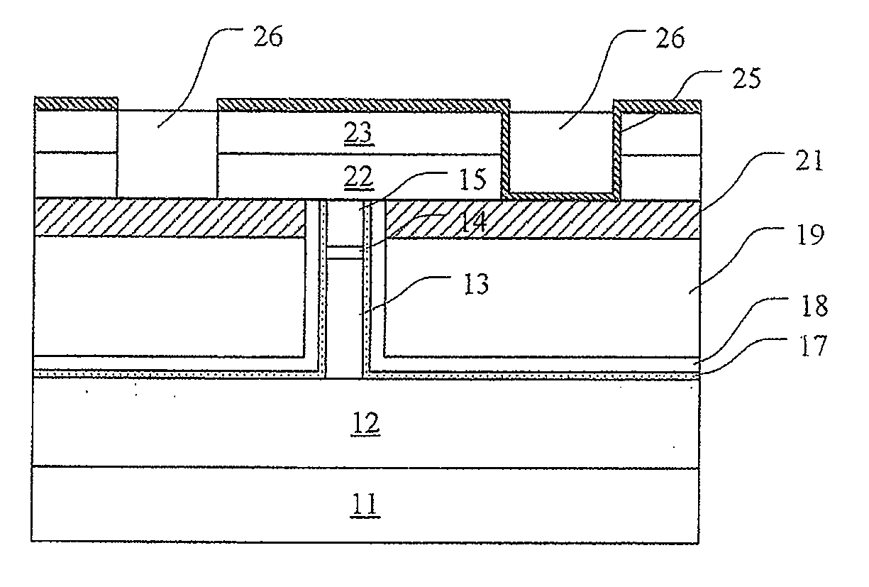
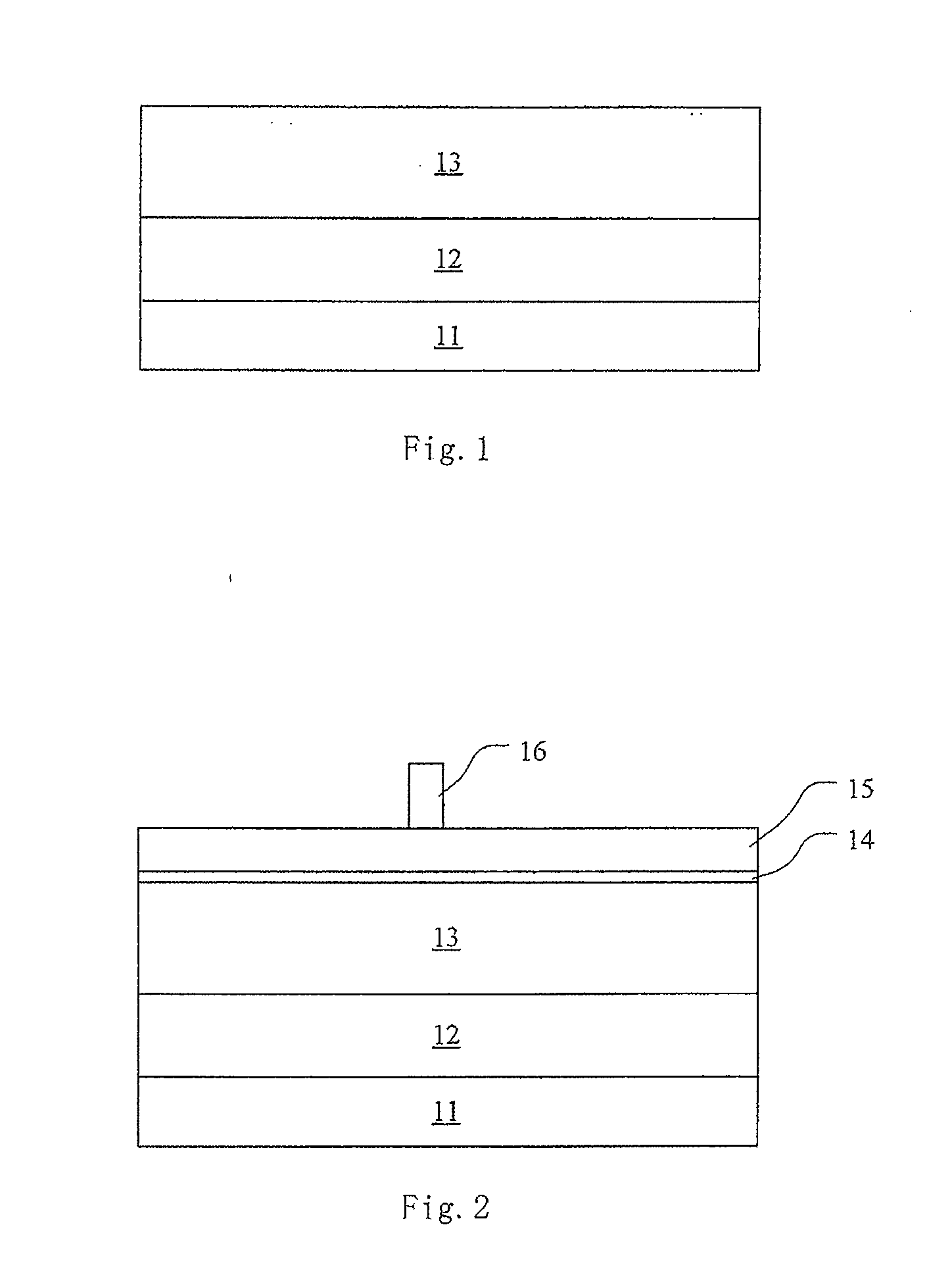
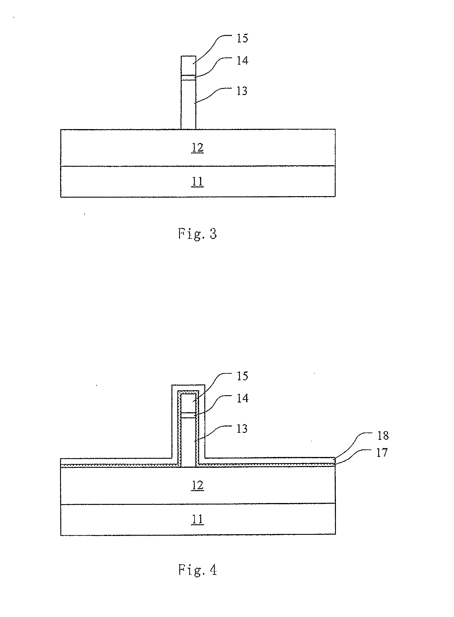
[0056]The non-volatile memory device according to the present invention is shown in FIGS. 15A and 15B, comprising: a fin formed from the top semiconductor layer 13 of the SOI wafer; source / drain regions (not shown) formed on both sides of the fin; a floating gate formed at one side of the fin and extending along the direction further away from the semiconductor fin, wherein the floating gate comprises the floating gate dielectric layer 17 and the floating gate conductor, the floating gate conductor being a stack of the conductive nitride 18 and the polysilicon layer 19; and a control gate covering the top and sidewall portions of the floating gate, wherein the control gate comprises a control gate conductor consisting of the intermediate dielectric layer 25 and the conductive filler.
second embodiment
[0057]The non-volatile memory device according to the present invention is shown in FIGS. 16A and 16B, comprising: a fin formed from the top semiconductor layer 13 on the SOI wafer; source / drain regions (not shown) formed on both sides of the fin; a floating gate formed at one side of the fin and extending in a direction further away from the semiconductor fin, wherein the floating gate comprises the floating gate dielectric layer 17 and the floating gate conductor, the floating gate conductor being a stack of the conductive nitride 18 and the polysilicon layer 19; and a control gate on top of the floating gate, wherein the control gate comprises a control gate conductor consisting of the intermediate dielectric layer 25 and the conductive filler 26.
[0058]The non-volatile memory device in the second embodiment differs from that in the first embodiment in that the control gate in the second embodiment is located only on top of the floating gate.
[0059]As a variation of the above non-v...
PUM
 Abstract
Description
Claims
Application Information
 - R&D Engineer
- R&D Manager
- IP Professional
- Industry Leading Data Capabilities
- Powerful AI technology
- Patent DNA Extraction
Browse by: Latest US Patents, China's latest patents, Technical Efficacy Thesaurus, Application Domain, Technology Topic, Popular Technical Reports.
© 2024 PatSnap. All rights reserved.Legal|Privacy policy|Modern Slavery Act Transparency Statement|Sitemap|About US| Contact US: help@patsnap.com