Optical module

a technology of optical modules and flexible printed circuits, applied in the association of printed circuit non-printed electric components, optical elements, instruments, etc., can solve the problems of inability to ensure the isolation between the lines, the wiring density of the flexible printed circuit becomes too high to physically arrange the wiring of the flexible printed circuit, and the conventional technology suffers, so as to reduce crosstalk and reduce the effect of wiring density

Active Publication Date: 2012-01-12
MITSUBISHI ELECTRIC CORP
View PDF6 Cites 4 Cited by
  • Summary
  • Abstract
  • Description
  • Claims
  • Application Information

AI Technical Summary

Benefits of technology

[0015]Therefore, the wiring density may be reduced without deterioration of the bending property of the flexible printed circuit, to thereby ensure the isolation between the lines to reduce crosstalk.

Problems solved by technology

However, the conventional technology suffers from the following problems.
This leads to a problem that the wiring density of the flexible printed circuit becomes too high to physically arrange the wiring of the flexible printed circuit.
For this reason, isolation between those lines cannot be ensured, resulting in problems that a signal in an adjacent channel produces crosstalk, and that an output signal crosses over into an input signal to oscillate.
This leads to another problem that the bending property of the flexible printed circuit is deteriorated to reduce the mounting property on the circuit board.

Method used


Image

  • Optical module
  • Optical module
  • Optical module

Examples


first embodiment

[0035

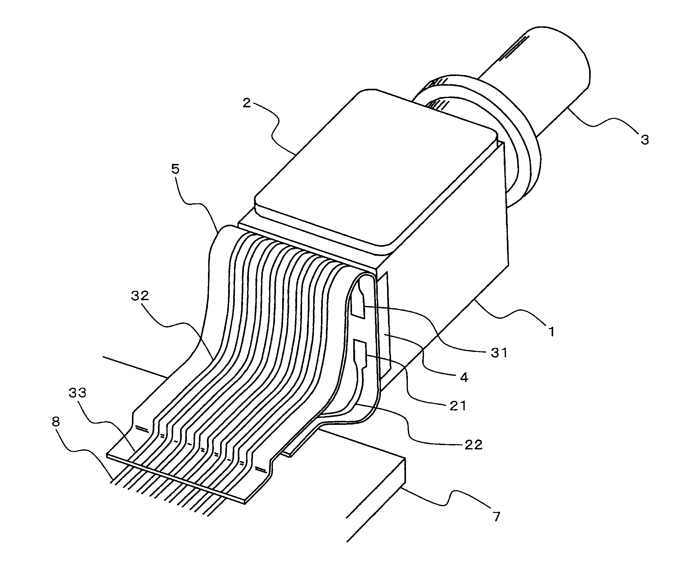
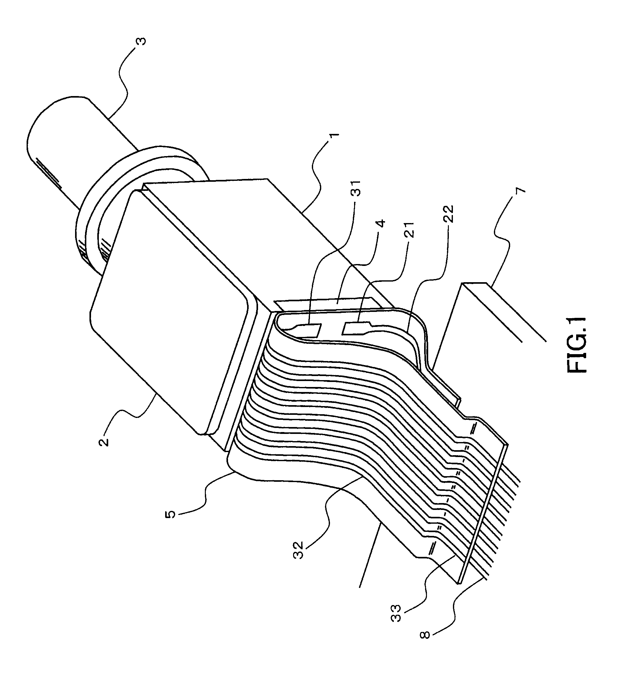
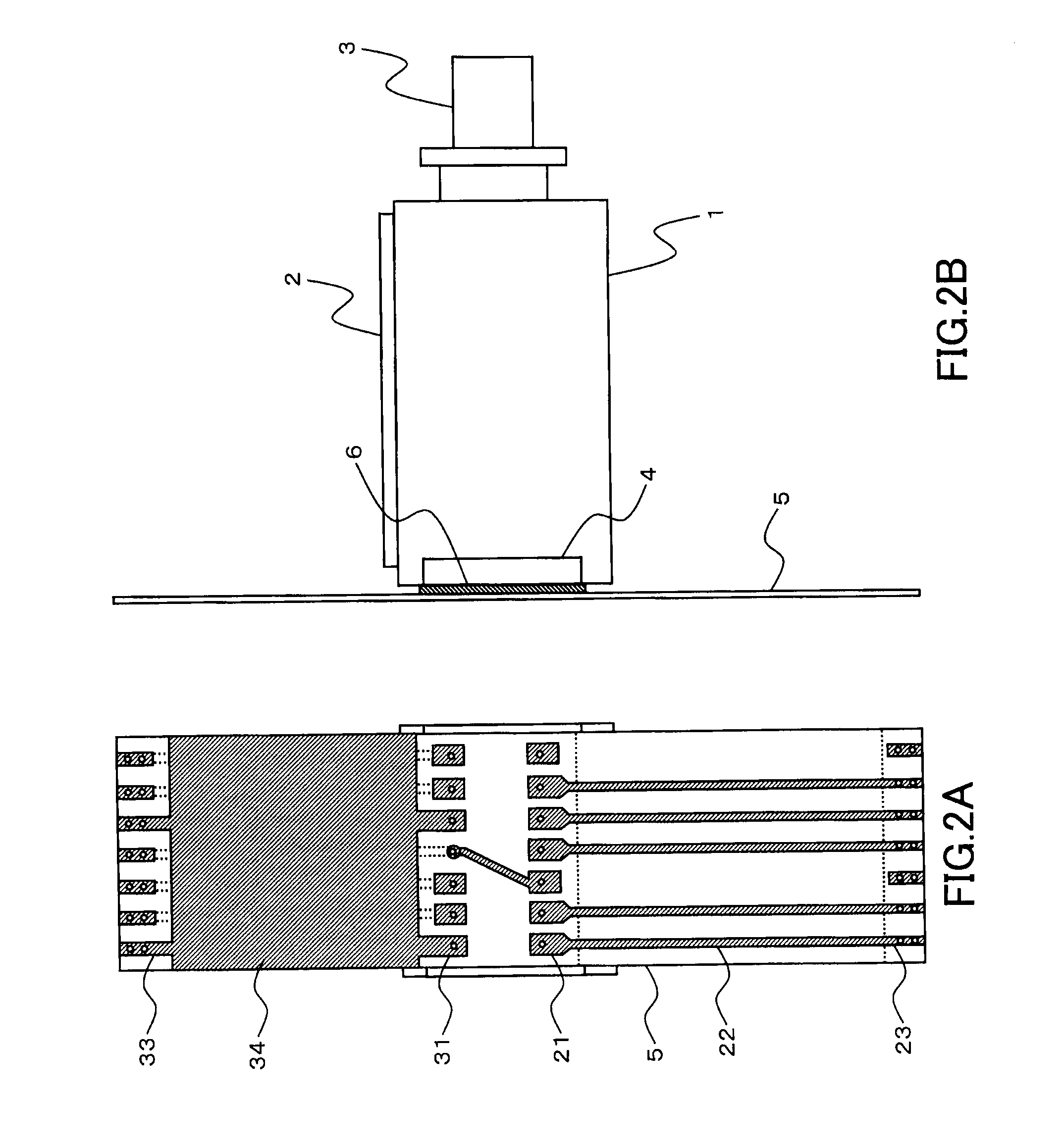
[0036]FIG. 1 is a perspective view illustrating an optical module according to a first embodiment of the present invention, together with a printed circuit board 7 (circuit board). FIG. 2A is a front view illustrating the optical module of FIG. 1, and FIG. 2B is a side view illustrating the optical module. FIG. 1 illustrates a state in which a flexible printed circuit 5 is bent for connection to the printed circuit board 7, and FIGS. 2A and 2B each illustrate a state before the optical module is connected to the printed circuit board 7, in which the flexible printed circuit 5 is not bent.

[0037]As illustrated in FIGS. 1, 2A, and 2B, the optical module includes a package 1, a cover 2 for the package 1, a receptacle 3, a feedthrough 4, and the flexible printed circuit 5.

[0038]The package 1 accommodates a carrier (not shown) having an optical device such as, for example, an optical modulator mounted thereon.

[0039]The receptacle 3 is disposed on one end side of the package 1, which ...

second embodiment

[0067

[0068]In the above-mentioned first embodiment, description has been given of the case in which the second ground conductor 34 is arranged between the first flexible printed circuit wiring patterns 22 and the second flexible printed circuit wiring patterns 32 to suppress the electromagnetic interference between the first flexible printed circuit wiring patterns 22 and the second flexible printed circuit wiring patterns 32. In a second embodiment, description is given of a configuration capable of suppressing the electromagnetic interference with respect to an external signal.

[0069]FIG. 4A is a front view illustrating a first wiring layer 16 of the flexible printed circuit 5 according to the second embodiment of the present invention, FIG. 4B is a front view transmissively illustrating a second wiring layer 17 of the flexible printed circuit 5, FIG. 4C is a front view transmissively illustrating a third wiring layer 18 of the flexible printed circuit 5, and FIG. 4D is a side view...

third embodiment

[0085

[0086]In the above-mentioned first and second embodiments, description has been give of the case in which the flexible printed circuit 5 is adhered to the feedthrough 4 with the anisotropically conductive adhesive 6. However, the present invention is not limited to this configuration. Alternatively, the flexible printed circuit 5 may be connected to the feedthrough 4 with the aid of a solder material. In a third embodiment, description is given of a configuration in which the flexible printed circuit 5 is connected to the feedthrough 4 with the aid of a solder material.

[0087]FIG. 5A is a front view illustrating the first wiring layer 12 of the flexible printed circuit 5 according to the third embodiment of the present invention, FIG. 5B is a front view transmissively illustrating the second wiring layer 13 of the flexible printed circuit 5, and FIG. 5C is a side view illustrating the flexible printed circuit 5.

[0088]As illustrated in FIGS. 5A and 5B, solder mounting holes 41 ar...


PUM


Abstract

Provided is an optical module in which wiring density may be reduced to ensure isolation between lines to reduce crosstalk. A flexible printed circuit includes: dielectric layers; a first pattern facing portion including a first ground conductor pattern and a first wiring pattern electrically connected to an electric terminal, which are facing each other through the dielectric layer; and a second pattern facing portion including a second ground conductor pattern and a second wiring pattern electrically connected to the electric terminal, which are facing each other through the dielectric layer, the second pattern facing portion facing the first pattern facing portion, in which when the dielectric layer is bent along a portion between the first pattern facing portion and the second pattern facing portion, at least one of the first ground conductor pattern and the second ground conductor pattern is located between the first wiring pattern and the second wiring pattern.

Description

BACKGROUND OF THE INVENTION[0001]1. Field of the Invention[0002]The present invention relates to an optical module for use in optical communication, and more particularly, to an optical module that is electrically connected through a flexible printed circuit to a circuit board for driving the optical module.[0003]2. Description of the Related Art[0004]A conventional optical module includes a package that accommodates a carrier on which an optical device is mounted, an optical connector that is disposed on one end of the package, a feedthrough that is disposed on the other end of the package, and a flexible printed circuit that is fixed to the feedthrough (for example, see JP 2007-71980 A).[0005]The feedthrough is formed of laminated ceramic, and has electric terminals (radio-frequency terminal and bias terminal) which are disposed on an outer surface of the package perpendicularly to an optical axis of input / output light to / from an optical connector, and a carrier connection termina...

Claims


Application Information

Patent Timeline
Patent Type & Authority Applications(United States)
IPC IPC(8): H05K1/18
CPCG02B6/4281G02B6/4292H05K2201/10121H05K1/028H05K1/189H05K1/0219H05K1/147H05K3/363H05K2201/055
Inventor ARUGA, HIROSHIOHASHI, HIDEYUKI
Owner MITSUBISHI ELECTRIC CORP
Why Eureka
Try Eureka