Electrophoretic display device and method of fabricating the same

a technology of electrophoretic display and substrate, which is applied in the field of electrophoretic display device, can solve the problems of driving error, difficult to accurately align the electrophoretic layer with the unit pixel, and the inability to fabricate the epd device according to the related art, and achieves high brightness and contrast ratio, enhanced contrast ratio, and high clarity

Active Publication Date: 2012-01-19
E INK CORPORATION
View PDF8 Cites 12 Cited by
  • Summary
  • Abstract
  • Description
  • Claims
  • Application Information

AI Technical Summary

Benefits of technology

[0026]An advantage of the present invention is to provide an electrophorectic display device without a color filter layer that can realize colors with high brightness and contrast ratio, and a method for fabricating the same.
[0027]Another advantage of the present invention is to provide an electrophoretic display device capable of enhancing a contrast ratio by displaying a black color of higher clarity, and a method for fabricating the same.
[0028]Still another advantage of the present invention is to provide an electrophoretic display device capable of reducing the fabrication costs and simplifying the fabrication process by directly forming an electrophoretic layer on a substrate where thin film transistors (TFTs) are formed, and a method for fabricating the same.
[0029]Additional features and advantages of the invention will be set forth in the description which follows, and in part will be apparent from the description, or may be learned by practice of the invention. These and other advantages of the invention will be realized and attained by the structure particularly pointed out in the written description and claims hereof as well as the appended drawings.
[0030]To achieve these and other advantages and in accordance with the purpose of the present invention, as embodied and broadly described, an electrophoretic display (EPD) device may include first and second substrates having a plurality of unit pixels, each unit pixel including three sub-pixels; a thin film transistor in each sub-pixel on the first substrate; a pixel electrode connected to a drain electrode of the thin film transistor; an electrophoretic layer on the pixel electrode, the electrophoretic layer including white charged particles, black charged particles and color charged particles; and a common electrode on the second substrate.
[0031]In another aspect of the present invention, a method of manufacturing an electrophoretic display (EPD) device, the EPD device having a plurality of unit pixels, each unit pixel including three sub-pixels, the method may include forming a thin film transistor in each sub-pixel on a first substrate; forming a passivation layer on the thin film transistor; forming a contact hole in the passivation layer; forming a pixel electrode on the passivation layer, the pixel electrode being connected to a drain electrode of the thin film transistor via the contact hole; forming a partition wall between the sub-pixels, the partition wall substantially surrounding the pixel electrode in each sub-pixel; forming an electrophoretic layer on the pixel electrode, the electrophoretic layer including white charged particles, black charged particles and color charged particles; and attaching the first substrate to a second substrate.

Problems solved by technology

First, the method of fabricating the EPD device according to the related art has difficulty in attaching the first substrate and the second substrate to each other.
However, the unit pixel of the EPD device is typically formed with a small size less than 150 micrometer in the height and width thereof, and thus it may be difficult to accurately align the electrophoretic layer with the unit pixel.
If the electrophoretic layer is not accurately aligned with the first substrate formed with a thin-film transistor, then an electric field is not accurately delivered to electrophoretic particles, thereby causing a driving error.
Second, the method of fabricating the EPD device according to the related art has a complicated fabrication process.
The first substrate 20 and the second substrate 40 are separately fabricated through different processes and transferred by a transfer means to be attached to each other in an attachment process, and thus it may be difficult to utilize an in-line fabrication process.
Third, electrostatic discharge generated during the process of attaching the first substrate 20 and second substrate 40 may cause failure in the initial alignment of electrophoretic particles.
In this case, electrostatic discharge generated during the process of peeling off the protection film may cause misalignment in the initial alignment of electrophoretic particles.
The misalignment of electrophoretic particles may generate a moire defect with a comb-tooth-shaped pattern during the operation of the EPD device.
Fourth, the EPD device according to the related has a deteriorated brightness and contrast ratio.

Method used


Image

  • Electrophoretic display device and method of fabricating the same
  • Electrophoretic display device and method of fabricating the same
  • Electrophoretic display device and method of fabricating the same

Examples


first embodiment

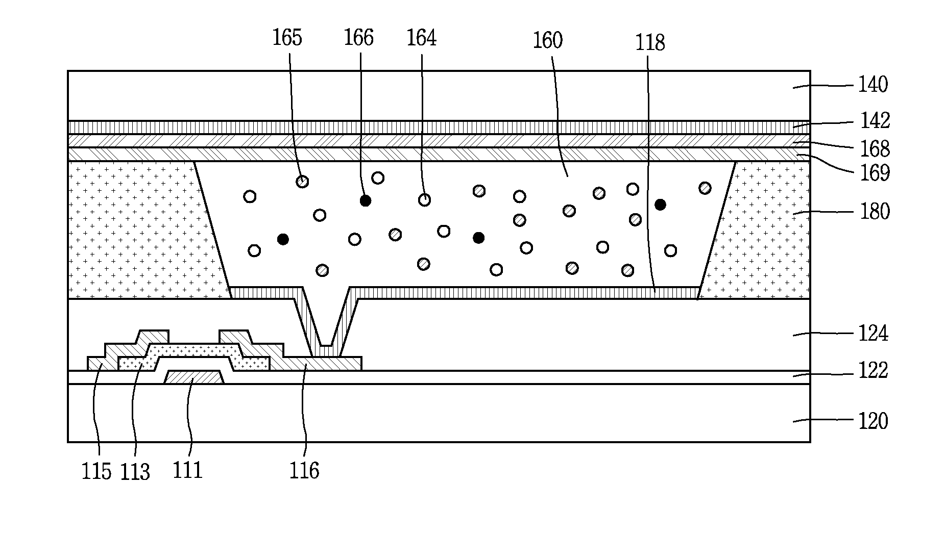
[0050]FIG. 2 is a cross-sectional view illustrating a structure of an EPD device according to the present invention. In the EPD device, a plurality of sub-pixels of cyan, magenta and yellow, or a plurality of sub-pixels of red, green and blue (RGB) are repeatedly arranged. However, only one sub-pixel will be hereinafter explained for convenience. The sub-pixels of cyan, magenta and yellow, or the sub-pixels of RGB constitute a unit pixel.

[0051]As illustrated in FIG. 2, the EPD device includes a first substrate 120 having a display region where a plurality of sub-pixels are arranged and a non-display region formed on an outer periphery of the display region, a second substrate 140 corresponding to the first substrate 120, a thin film transistor (TFT) formed on each sub-pixel on the first substrate 120, a passivation layer 124 formed on the first substrate 120 where the TFTs have been formed, a pixel electrode 118 formed on each sub-pixel on the passivation layer 124, a partition wall...

second embodiment

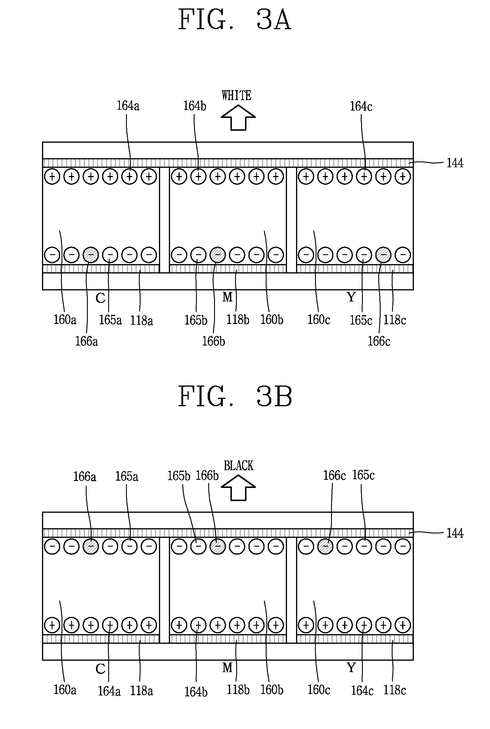
[0113]FIGS. 7A and 7B are views illustrating a method for implementing colors on an electrophoretic display device according to the present invention.

[0114]In this embodiment, the pixel includes four sub-pixels having the cyan sub-pixel, the magenta sub-pixel, the yellow sub-pixel, and a white sub-pixel or four sub-pixels having the cyan sub-pixel, the magenta sub-pixel, the yellow sub-pixel, and a black sub-pixel. The white sub-pixel improves the brightness of the EPD device and the black sub-pixel improves the contrast ratio of the EPD device.

[0115]As shown in FIG. 7A, the EPD device includes having the cyan sub-pixel, the magenta sub-pixel, the yellow sub-pixel, and a white sub-pixel. In the cyan sub-pixel C, the magenta sub-pixel M, and the yellow sub-pixel Y, the cyan color particles 165a, the magenta particles 165b, the yellow particles 165c, the black particles 166a,166b,166c, and the white particles 164a,164b,164c are respectively filled. In the white sub-pixel, only the whi...


PUM

PropertyMeasurementUnit
volume ratioaaaaaaaaaa
sizeaaaaaaaaaa

Abstract

Disclosed is an electrophoretic display (EPD) device capable of implementing colors with high brightness. Each sub-pixel implement colors with driving color particles, white particles and black particles, and the EPD device has an enhanced contrast ratio due to black particles.

Description

[0001]This application claims the benefit of Korean Patent Application No. 10-2010-0068127, filed on Jul. 14, 2010, which is hereby incorporated by reference for all purposes as if fully set forth herein.BACKGROUND OF THE INVENTION[0002]1. Field of the Invention[0003]The present invention relates to an electrophoretic display (EPD) device and a method for fabricating the same, and more particularly to an EPD device with enhanced brightness and contrast ratio, reduced fabrication costs and short fabrication time, and a method for fabricating the same.[0004]2. Discussion of the Related Art[0005]An electrophoretic display (EPD) device is an image display device using a phenomenon that colloidal particles move to either one of the polarities when one pair of electrodes to which a voltage is applied are immersed into a colloidal solution. Compared to a liquid crystal display (LCD) device, such an EPD device has the advantages of wide viewing angle, high reflectivity, low power consumptio...

Claims


Application Information

Patent Timeline
Patent Type & Authority Applications(United States)
IPC IPC(8): G02F1/167H01L33/50G02F1/16766G02F1/1679
CPCG02F1/167G02F2001/1676G02F2001/1672G02F1/1681G02F1/16766G02F1/1679G02F1/1676
Inventor PARK, CHOON-HOPAEK, SEUNG-HANSHIN, SANG-IL
Owner E INK CORPORATION
Why Eureka
Try Eureka