Active chip on carrier or laminated chip having microelectronic element embedded therein
a technology of active chips and laminated chips, applied in the field of microelectronic elements, can solve the problems of not being able to reduce the volume occupied, the thinning process cannot continue without limit,
- Summary
- Abstract
- Description
- Claims
- Application Information
AI Technical Summary
Benefits of technology
Problems solved by technology
Method used
Image


Examples
Embodiment Construction
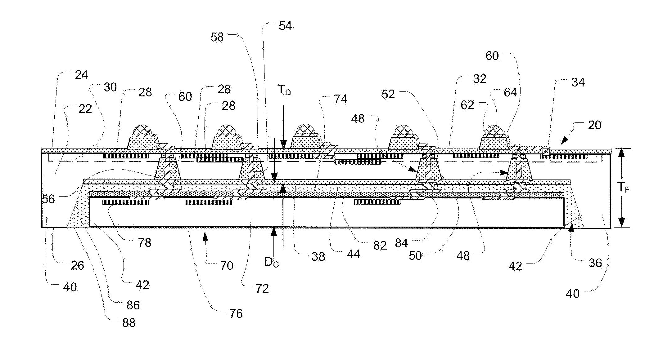
[0028]A microelectronic structure according to one embodiment of the invention (FIG. 1) includes a first semiconductor chip 20 having a body 22 with a front surface 24 facing in a forward direction, toward the top of the drawing in FIG. 1, and a rear surface 26 facing in the opposite, rearward direction. Rear surface 26 is generally parallel to front surface 24. The directions parallel to front surface 24 are referred to herein as “horizontal” directions, and are also referred to herein as the “X” and “Y” directions; whereas the directions perpendicular to the front surface are referred to herein as the forward and rearward directions, and are also referred to herein as the “vertical” or “Z” directions. The directions referred to herein are in the frame of reference of the structures referred to. Thus, these directions may lie at any orientation in the normal or gravitational frame of reference. Body 22 includes active circuit elements schematically represented at 28 in FIG. 1. Acti...
PUM
 Abstract
Description
Claims
Application Information