Cooling structure of capacitor and inverter device

a cooling structure and capacitor technology, applied in the field of capacitors, can solve the problems of mechanical stress, insufficient reliability of the capacitor, cracks in the laminated ceramic capacitor, etc., and achieve the effect of suppressing the temperature rise of the capacitor and improving reliability

Inactive Publication Date: 2012-01-26
MITSUBISHI ELECTRIC CORP
View PDF8 Cites 26 Cited by
  • Summary
  • Abstract
  • Description
  • Claims
  • Application Information

AI Technical Summary

Benefits of technology

[0021]The present invention has been made to solve the foregoing problem, and an object of the present invention is to provide a cooling structure of a capacitor consisting of a ceramic electronic component in which lead terminals are joined to external electrodes to improve reliability by suppressing the temperature rise of the capacitor.
[0026]According to the present invention, an insulating member having a high coefficient of thermal conductivity is provided between a capacitor consisting of a laminated ceramic electronic component in which lead terminals are joined to external electrodes and a heat dissipation plate or a circuit board to dissipate the heat derived from the capacitor by paths together with heat dissipation paths of the lead terminals and the electrically-conducting paths; whereby, the temperature rise of the capacitor is suppressed, the capacitor can be used for long periods, and reliability can be improved.
[0027]Furthermore, a cooling structure of a snubber capacitor to be connected in parallel to semiconductor switching elements of an inverter circuit is used; whereby, an inverter device with high reliability can be provided.

Problems solved by technology

However, as in the inverter device for use in an automobile, mechanical stress is generated due to the difference of coefficients of thermal expansion between the laminated ceramic capacitor and a circuit board to which the laminated ceramic capacitor is mounted in circumstances whose temperature change and temperature cycle are large; and accordingly, a crack may be generated in the laminated ceramic capacitor.
More particularly, in the case where a metal circuit board serving as a high heat dissipation substrate has a large coefficient of thermal expansion and the laminated ceramic capacitor is mounted on the metal circuit board, a problem exists in that the occurrence of the crack caused by the difference of the coefficients of thermal expansion becomes prominent and accordingly reliability of the capacitor cannot be sufficiently kept.
By the way, in an inverter device having a large current of several hundred amperes and high speed switching, a peak current generated by a surge voltage is large and self-heating of a snubber capacitor to which the peak current flows cannot be negligible.
However, in the case where the conventional laminated ceramic capacitors 1a, 1b, and 1c shown in FIG. 7 to FIG. 9, whose mechanical stresses are reduced, are mounted as the snubber capacitors, paths through which the heat is dissipated to the metal substrate are limited to the lead terminals and the electrically-conducting paths.
If the coefficient of thermal conductivity and the thickness of material for use in the lead terminal and the electrically-conducting path are not sufficient, the heat generated in the snubber capacitor is not sufficiently dissipated to the substrate side; and accordingly, the temperature of the laminated ceramic capacitor rises.
Therefore, a problem exists in that the temperature rise of the capacitor shortens operating life of the capacitor and reduces reliability thereof.
The paths through which the heat is dissipated to the cooling fin are originally limited to the capacitor electrode and the conductor; and therefore, a problem exists in that if the coefficients of thermal conductivity of the material for use in the capacitor electrode and the conductor are not sufficient, the heat generated by the snubber capacitor is not still dissipated sufficiently to the cooling fin side and accordingly the temperature of the snubber capacitor rises.

Method used


Image

  • Cooling structure of capacitor and inverter device
  • Cooling structure of capacitor and inverter device
  • Cooling structure of capacitor and inverter device

Examples


embodiment 1

Preferred Embodiment 1

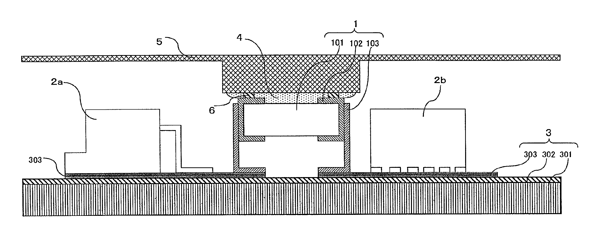
[0038]Hereinafter, a cooling structure of a capacitor and an inverter device according to a preferred embodiment 1 of the present invention will be described with reference to FIG. 1.

[0039]FIG. 1 is a schematic side view showing the configuration of the cooling structure of the capacitor and the inverter device using the cooling structure of the capacitor and, in this case, the schematic side view shows only a U phase of an inverter circuit as a representative. Furthermore, an actual inverter device includes a heat sink and an inverter case; however, in this case, the heat sink and the inverter case are not shown.

[0040]As shown in FIG. 1, in the inverter device according to the preferred embodiment 1, a snubber capacitor 1 and semiconductor switching elements 2a and 2b of upper and lower arms of the inverter circuit are mounted on a metal circuit board 3. The semiconductor switching elements 2a and 2b and other semiconductor switching elements of V phase and W ...

embodiment 2

Preferred Embodiment 2

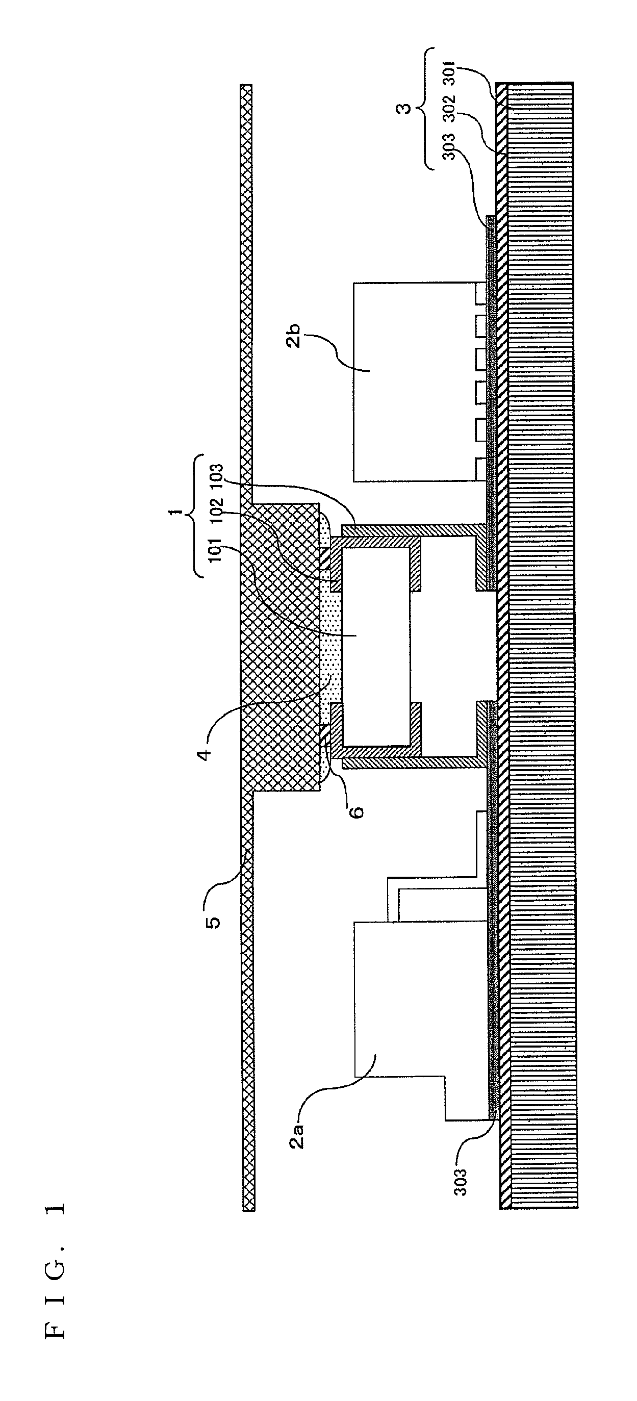
[0048]Next, a cooling structure of a capacitor and an inverter device according to a preferred embodiment 2 of the present invention will be described with reference to FIG. 2.

[0049]FIG. 2 is a schematic side view showing the configuration of the cooling structure of the capacitor and the inverter device using the cooling structure of the capacitor and, in this case, as in FIG. 1, the schematic side view shows only a U phase of an inverter circuit as a representative. Furthermore, an actual inverter device includes a heat sink and an inverter case; however, in this case, the heat sink and the inverter case are not shown. Incidentally, in FIG. 2, the same reference numerals are given to those identical to or equivalent to constituent elements in the preferred embodiment 1 shown in FIG. 1.

[0050]The preferred embodiment 2 is different from the preferred embodiment 1 on the points that a heat dissipation plate 5 is extended and the ends thereof and a metal base pla...

embodiment 3

Preferred Embodiment 3

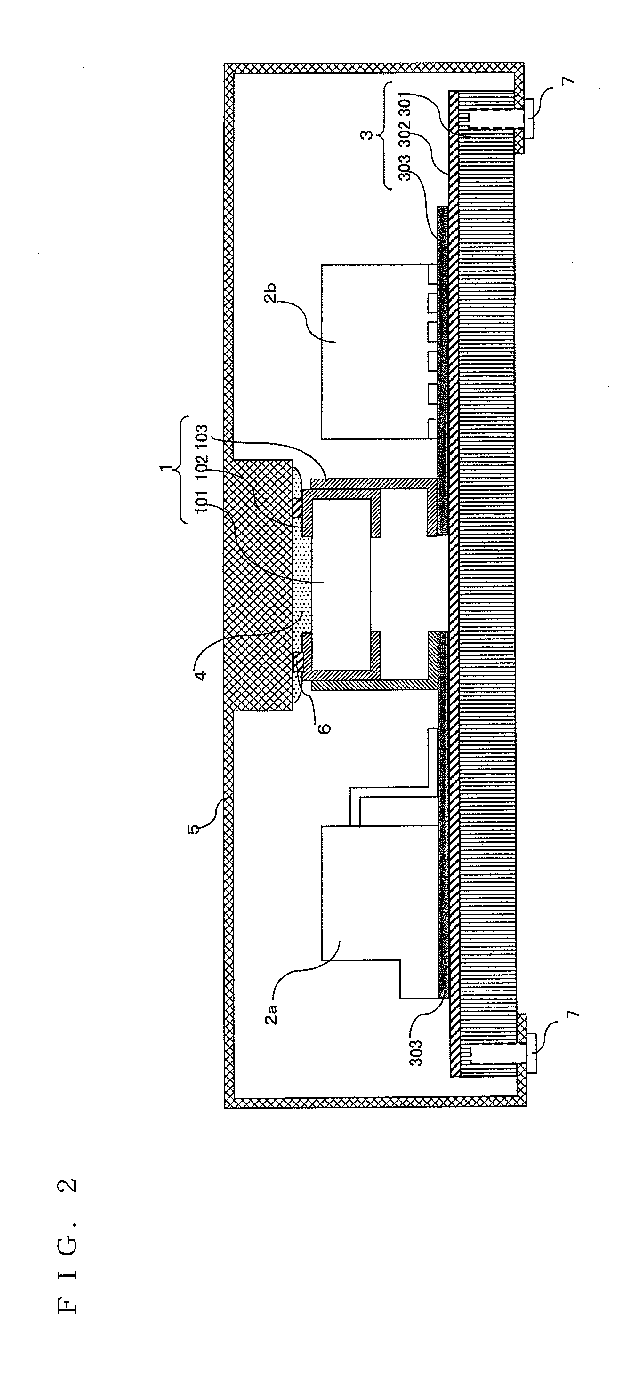
[0052]Next, a cooling structure of a capacitor and an inverter device according to a preferred embodiment 3 of the present invention will be described with reference to FIG. 3.

[0053]FIG. 3 is a schematic side view showing the configuration of the cooling structure of the capacitor and the inverter device using the cooling structure of the capacitor and, in this case, as in FIG. 1, the schematic side view shows only a U phase of an inverter circuit as a representative. Incidentally, in FIG. 3, the same reference numerals are given to those identical to or equivalent to constituent elements in the preferred embodiment 1 shown in FIG. 1.

[0054]In the preferred embodiment 3, a snubber capacitor 1 and semiconductor switching elements 2a and 2b that constitute the inverter circuit are mounted on a circuit board 3 and the thus configured snubber capacitor 1 and inverter circuit are covered with an inverter case 8 that is an outer covering; and the inverter case 8 serve...


PUM


Abstract

A cooling structure of a capacitor includes a snubber capacitor in which lead terminals are joined to external electrodes of a laminated ceramic electronic component; a circuit board which is for mounting the snubber capacitor and semiconductor switching elements; and a heat dissipation plate which is made of metal that dissipates the heat generated in the circuit board. The cooling structure of the capacitor is configured such that an insulating member having a high coefficient of thermal conductivity intervenes between the snubber capacitor and the heat dissipation plate.

Description

BACKGROUND OF THE INVENTION[0001]1. Field of the Invention[0002]The present invention relates to capacitors consisting of ceramic electronic components to be mounted on circuit boards and, more particularly, relates to a cooling structure of a snubber capacitor and an inverter device using the cooling structure of the capacitor.[0003]2. Description of the Related Art[0004]In recent years, motors equipped with inverters have become widespread from the flow of energy saving. FIG. 6 is an example of a circuit diagram of a three phase inverter which is for driving a motor 12. As shown in the drawing, a plurality of semiconductor switching elements 2 (when named generically, additional characters will not be repeated later), each of the plurality of semiconductor switching elements 2 consisting of a corresponding one of semiconductor switching elements 2a, 2c, and 2e on the upper arm side and a corresponding one of semiconductor switching elements 2b, 2d, and 2f on the lower arm side, ar...

Claims


Application Information

Patent Timeline
Patent Type & Authority Applications(United States)
IPC IPC(8): H05K7/20H02M1/00
CPCH01G2/08H02P2201/00Y02B70/1491H01G4/228H02M2001/346H05K7/209H02M1/346Y02B70/10
Inventor SOTOME, HIDEYUKI
Owner MITSUBISHI ELECTRIC CORP
Why Eureka
Try Eureka