Method of preparing carbon thin film, electronics comprising carbon thin film, and electrochemical device comprising carbon thin film

a technology of carbon thin film and carbon thin film, which is applied in the direction of single-layer graphene, cell components, sustainable manufacturing/processing, etc., can solve the problem of limited use of graphite in the semiconductor industry

Inactive Publication Date: 2012-01-26
POSTECH ACAD IND FOUND
View PDF8 Cites 47 Cited by
  • Summary
  • Abstract
  • Description
  • Claims
  • Application Information

AI Technical Summary

Benefits of technology

[0007]The present invention provides a method of preparing a cos...

Problems solved by technology

Due to electrical conductivity similar to that of metal,...

Method used


Image

  • Method of preparing carbon thin film, electronics comprising carbon thin film, and electrochemical device comprising carbon thin film
  • Method of preparing carbon thin film, electronics comprising carbon thin film, and electrochemical device comprising carbon thin film
  • Method of preparing carbon thin film, electronics comprising carbon thin film, and electrochemical device comprising carbon thin film

Examples


example 1

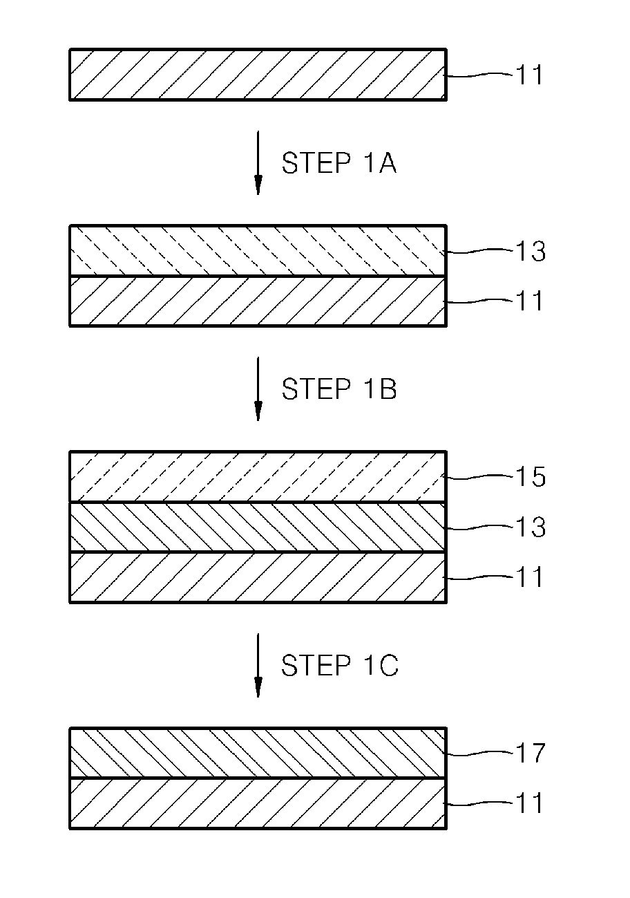
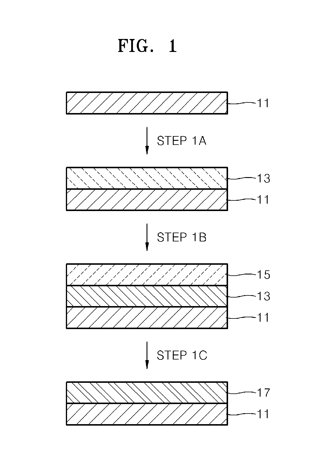
[0165]A silicon substrate (2.0 cm×2.0 cm) on which a silicon oxide layer having a thickness of 300 nm is formed was prepared and the surface of the silicon oxide layer was hydrophilically modified by treating the surface of the silicon oxide layer with UV light / ozone for 30 minutes.

[0166]A 2 wt % solution prepared by dissolving polystyrene (weight average molecular weight (Mw): 130000 g / mol, manufactured by Sigma-Aldrich) in dimethylformamide (DMF, manufactured by DAE JUNG Chemicals) solvent was spin coated on the silicon oxide layer, and baked at 100° C. for 3 minutes to remove the solvent, resulting in forming a polystyrene layer having a thickness of 10 nm.

[0167]Nickel (Ni) was deposited on the polystyrene layer to form a Ni protective layer having a thickness of 50 nm, and then the substrate was disposed in a quartz tube and installed in a furnace. The substrate was heat-treated at 1000° C. for 1 minute using a halogen lamp heat source while uniformly flowing argon (Ar) gas (50 ...

example 2

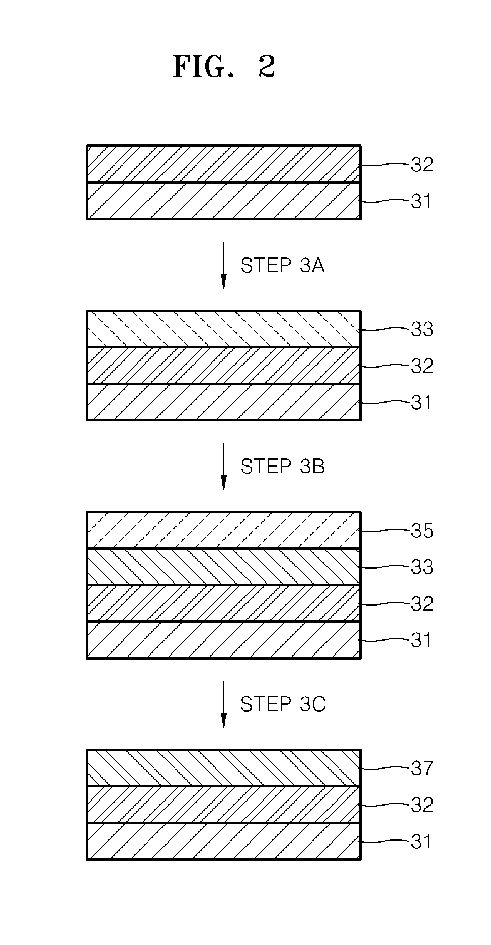
[0169]A carbon thin film was obtained in the same manner as in Example 1, except that polyacrylonitrile (weight average molecular weight (Mw): 150000 g / mol, manufactured by Sigma-Aldrich) was used instead of the polystyrene. Conductivity of the carbon thin film measured using a 4-point probe was 100 S / cm.

example 3

[0170]A carbon thin film was obtained in the same manner as in Example 1, except that polymethyl methacrylate (number average molecular weight (Mn): 130000 g / mol) was used instead of the polystyrene. Conductivity of the carbon thin film measured using a 4-point probe was 105 S / cm.


PUM

PropertyMeasurementUnit
Temperatureaaaaaaaaaa
Timeaaaaaaaaaa

Abstract

A method of preparing a carbon thin film, and electronics including the carbon thin film.

Description

CROSS-REFERENCE TO RELATED PATENT APPLICATION[0001]This application claims the benefit of Korean Patent Application No. 10-2010-0071062, filed on Jul. 22, 2010, and Korean Patent Application No. 10-2011-0070032, filed on Jul. 14, 2011, in the Korean Intellectual Property Office, the disclosures of which are incorporated herein in their entirety by reference.BACKGROUND OF THE INVENTION[0002]1. Field of the Invention[0003]The present invention relates to a method of preparing a carbon thin film, electronics including the carbon thin film, and an electrochemical device including the carbon thin film.[0004]2. Description of the Related Art[0005]In general, carbonaceous materials may be classified into diamond, graphite, graphene, a-few-layer graphene (FLG), and amorphous carbon. While, diamond does not have electrical conductivity because its carbon atoms are connected to each other by sp3 bonds, graphite has excellent electrical conductivity since its carbon atoms are connected to each...

Claims


Application Information

Patent Timeline
IPC IPC(8): B32B27/00B05D3/02
CPCB82Y30/00Y02E60/122C01B31/02C01B31/04C01B31/0446C01B2204/02C01B2204/04C01P2002/02C01P2006/40H01L51/0021H01L51/5203H01M4/583H01M4/8605H01M8/0234Y02E60/50Y02E10/549B82Y40/00C01B32/05C01B32/184C01B32/21Y02P70/50Y02E60/10H10K71/60H10K50/805H10K50/88
Inventor LEE, TAE-WOOCHOI, HEE CHEULBYUN, SUN JUNG
Owner POSTECH ACAD IND FOUND
Why Eureka
Try Eureka