Film for semiconductor device production, method for producing film for semiconductor device production, and method for semiconductor device production

a technology for semiconductor devices and production methods, applied in semiconductor/solid-state device details, identification means, instruments, etc., can solve problems such as the inability to separate adhesive layer-attached dicing tape from the separator well

Active Publication Date: 2012-02-02
NITTO DENKO CORP
View PDF2 Cites 11 Cited by
  • Summary
  • Abstract
  • Description
  • Claims
  • Application Information

AI Technical Summary

Benefits of technology

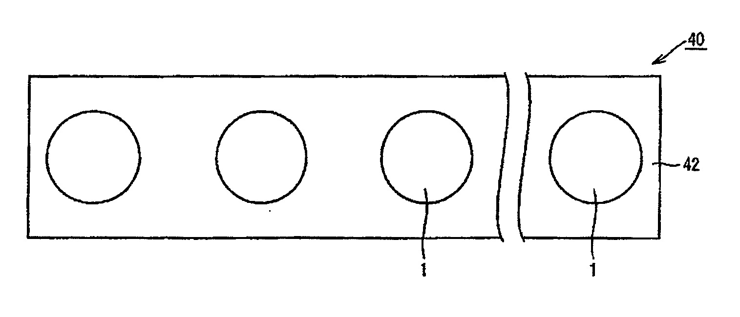
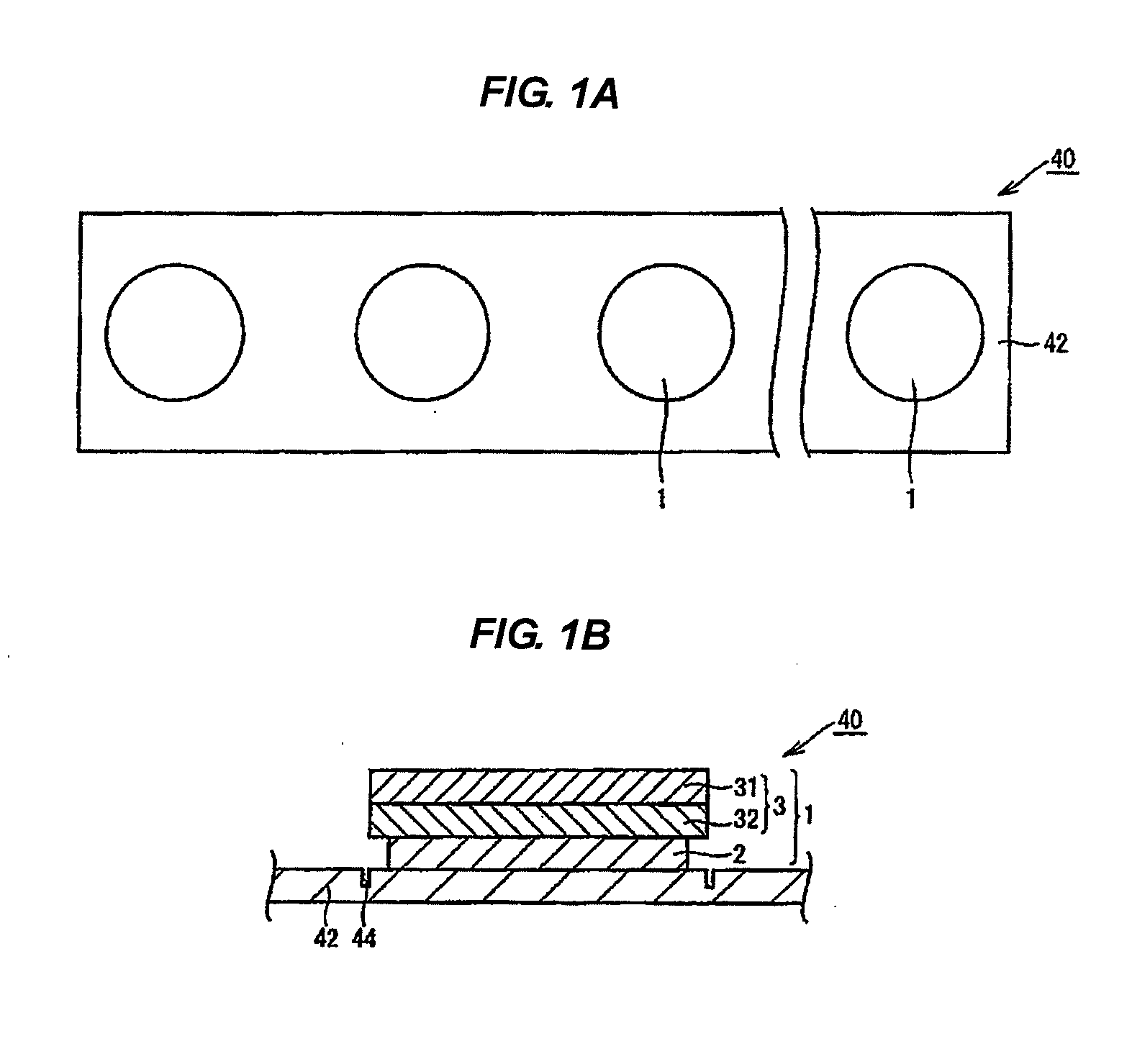
[0018]According to the above-mentioned constitution, the separator is so processed as to have a cut formed along the outer periphery of the dicing tape. Accordingly, starting from the cut, the adhesive layer-attached dicing tape can be easily peeled from the separator. Since the depth of the cut (cutting depth) is at most ⅔ of the thickness of the separator, the separator is prevented from being torn from the cut part (cut) when the adhesive layer-attached dicing tape is peeled from the separator. As a result, the adhesive layer-attached dicing tape can be favorably peeled (picked up) from the separator. Herein, the term “cut” in this specification means a part where the separator is cut to a certain depth not exceeding the thickness of the separator. The term “cut” may be referred to as “groove”.
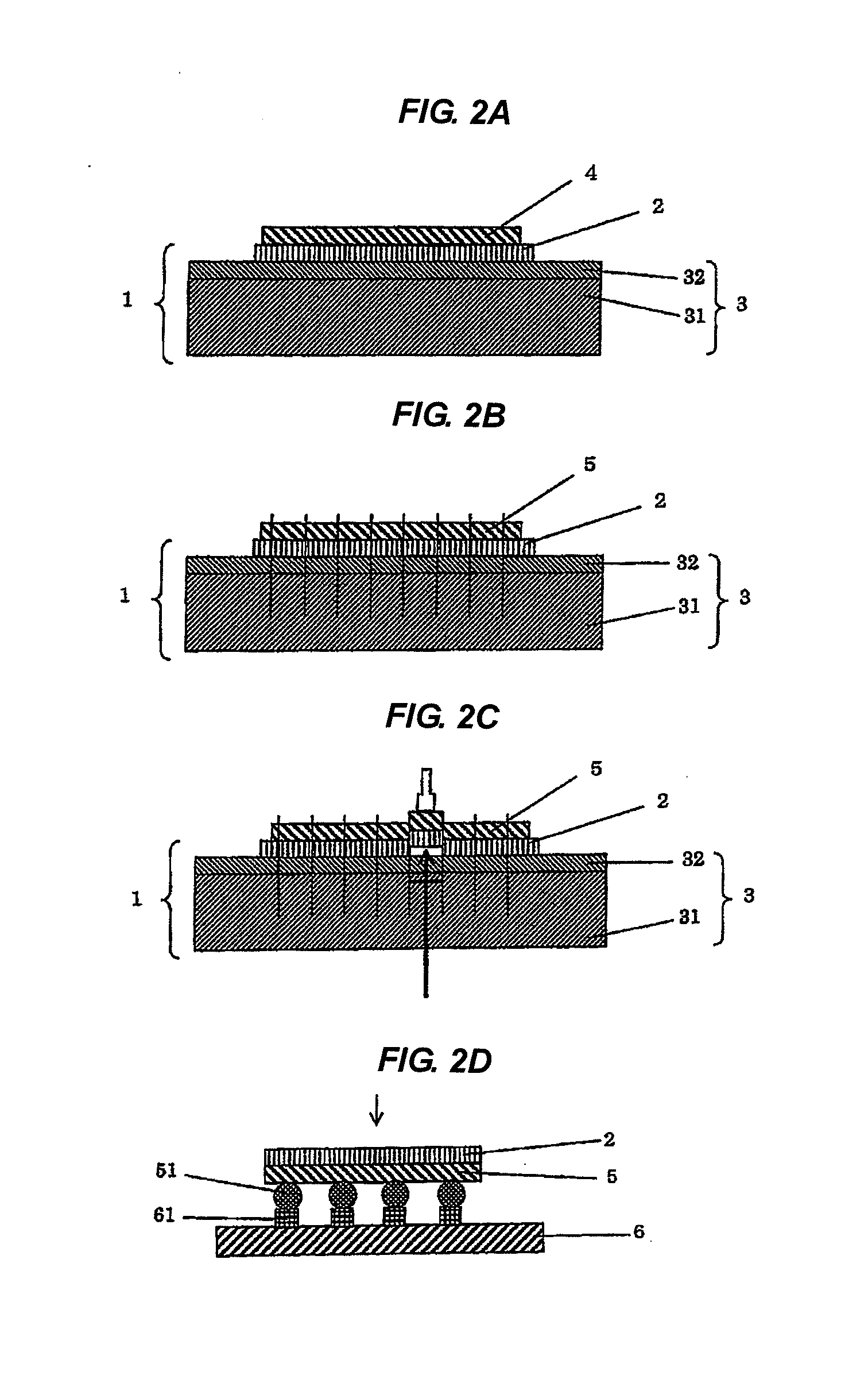
[0020]According to the above-mentioned constitution, when the separator-attached film is cut in accordance with the size corresponding to the semiconductor wafer to which the film is stuck, the film is cut to the depth of at most ⅔ of the thickness of the separator from the dicing tape side. As a result, in the film for semiconductor device production to be produced, the separator is so processed as to have a cut formed along the outer periphery of the dicing tape, and the depth of the cut is at most ⅔ of the thickness of the separator. Accordingly, in the film for semiconductor device production to be produced according to the production method for producing a semiconductor device production of the invention, the adhesive layer-attached dicing tape can be readily peeled from the separator starting from the cut. In addition, since the depth of the cut is at most ⅔ of the thickness of the separator, the separator is prevented from being torn from the cut part (cut) when the adhesive layer-attached dicing tape is peeled from the separator. As a result, the adhesive layer-attached dicing tape can be favorably peeled (picked up) from the separator.
[0022]The semiconductor device production method of the invention uses the above-mentioned film for semiconductor device production, in which the depth of the cut formed in the separator is at most ⅔ of the thickness of the separator. Accordingly, the separator is prevented from being torn from the cut part (cut) when the adhesive layer-attached dicing tape is peeled from the separator, and a semiconductor wafer can be favorably stuck onto the adhesive layer.
[0024]In the above-mentioned constitution, the separator is so processed as to have a cut formed along the outer periphery of the dicing tape. Accordingly, starting from the cut, the dicing tape can be readily peeled from the separator. In addition, since the depth of the cut is at most ⅔ of the thickness of the separator, the separator is prevented from being torn from the cut part (cut) when the dicing tape is peeled from the separator. As a result, the dicing tape can be favorably peeled (picked up) from the separator.
[0026]In the above constitution, when the separator-attached film is cut in accordance with the size corresponding to the semiconductor wafer to which the film is stuck, the film is cut to the depth of at most ⅔ of the thickness of the separator from the side of the dicing tape. As a result, in the film for semiconductor device production to be produced, the separator is so processed as to have a cut formed along the outer periphery of the dicing tape, and the depth of the cut is at most ⅔ of the thickness of the separator. Accordingly, in the film for semiconductor device production to be produced according to the production method for producing a film for semiconductor device production of the invention, the dicing tape can be readily peeled from the separator, starting from the cut. In addition, since the depth of the cut is at most ⅔ of the thickness of the separator, the separator is prevented from being torn from the cut part (cut) when the dicing tape is peeled from the separator. As a result, the dicing tape can be favorably peeled (picked up) from the separator.
[0028]The method for producing a semiconductor device of the invention uses the above-mentioned film for semiconductor device production, in which, therefore, the depth of the cut formed in the separator is at most ⅔ of the thickness of the separator. Accordingly, the separator is prevented from being torn from the cut part (cut) when the dicing tape is peeled from the separator, and a semiconductor wafer can be favorably stuck onto the adhesive layer.

Problems solved by technology

However, depending on the physical properties of the adhesive layer-attached dicing tape and on the condition of the apparatus, there has occurred an additional problem in that the adhesive layer-attached dicing tape could not be well separated from the separator.

Method used


Image

  • Film for semiconductor device production, method for producing film for semiconductor device production, and method for semiconductor device production
  • Film for semiconductor device production, method for producing film for semiconductor device production, and method for semiconductor device production
  • Film for semiconductor device production, method for producing film for semiconductor device production, and method for semiconductor device production

Examples


example 1

Preparation of Adhesive layer

[0160]113 parts of an epoxy resin (trade name “EPICOAT 1004” manufactured by JER Co., Ltd.), 121 parts of a phenolic resin (trade name “MILEX XLC-4L” manufactured by Mitsui Chemicals, Inc.), 246 parts of sphere silica (trade name “SO-25R” manufactured by Admatechs Co., Ltd.), 5 parts of Dye 1 (trade name “OIL GREEN 502” manufactured by Orient Chemical Industries Co., Ltd.), and 5 parts of Dye 2 (trade name “OIL BLACK BS” manufactured by Orient Chemical Industries Co., Ltd.) based on 100 parts of an acrylate-based polymer (trade name “PARACRON W-197CM” manufactured by Negami Chemical Industrial Co., Ltd.) containing ethyl acrylate and methyl methacrylate as main components were dissolved in methyl ethyl ketone to prepare a solution of a paste composition having a solid concentration of 23.6% by weight.

[0161]The solution of the paste composition was applied onto a separator of a polyethylene terephthalate film having a thickness of 50 μm, which had been su...

example 2

[0165]A film for semiconductor device production of Example 2 was prepared in the same manner as in Example 1, in which, however, the spacer was introduced so that the cutting depth in the separator in precutting could be 20 μm.


PUM

PropertyMeasurementUnit
thicknessaaaaaaaaaa
thicknessaaaaaaaaaa
thicknessaaaaaaaaaa

Abstract

The present invention relates to a film for semiconductor device production, which includes: a separator; and a plurality of adhesive layer-attached dicing tapes each including a dicing tape and an adhesive layer laminated on the dicing tape, which are laminated on the separator at a predetermined interval in such a manner that the adhesive layer attaches to the separator, in which the separator has a cut formed along the outer periphery of the dicing tape, and the depth of the cut is at most ⅔ of the thickness of the separator.

Description

FIELD OF THE INVENTION[0001]The present invention relates to a film for semiconductor device production, a method for producing a film for semiconductor device production, and a method for semiconductor device production.BACKGROUND OF THE INVENTION[0002]Recently, thinning and miniaturization of a semiconductor device and its package have been increasingly demanded. Therefore, as the semiconductor device and its package, flip chip type semiconductor devices in which a semiconductor element such as a semiconductor chip is mounted (flip chip-connected) on a substrate by means of flip chip bonding have been widely utilized. In such flip chip connection, a semiconductor chip is fixed to a substrate in a form where a circuit face of the semiconductor chip is opposed to an electrode-formed face of the substrate. In such a semiconductor device or the like, there may be a case where the back surface of the semiconductor chip is protected with a protective film to prevent the semiconductor ch...

Claims


Application Information

Patent Timeline
Patent Type & Authority Applications(United States)
IPC IPC(8): H01L21/02B32B38/04B32B38/10B65D65/28C09J7/20
CPCC09J7/02C09J2203/326H01L21/561H01L21/563H01L21/6835H01L23/293H01L23/3114H01L23/3164H01L23/544H01L24/13H01L24/16H01L24/27H01L24/29H01L24/81H01L24/83H01L24/92H01L2221/68336H01L2221/68377H01L2221/68381H01L2221/68386H01L2223/54406H01L2223/5442H01L2223/5448H01L2224/131H01L2224/16227H01L2224/16245H01L2224/27003H01L2224/27436H01L2224/2929H01L2224/293H01L2224/29386H01L2224/73204H01L2224/81095H01L2224/81191H01L2224/81815H01L2224/8191H01L2224/83191H01L2224/8385H01L2224/92H01L2224/92125H01L2924/01013H01L2924/01029H01L2924/0103H01L2924/01047H01L2924/0105H01L2924/01051H01L2924/01056H01L2924/01079H01L2924/01082H01L2224/2919H01L2924/01005H01L2924/01006H01L2924/0102H01L2924/01023H01L2924/01024H01L2924/01033H01L2924/01042H01L2924/01045H01L2924/01074H01L2924/01075H01L2924/014H01L2924/0665H01L2224/29101H01L2224/16225H01L2224/13111H01L2224/13144H01L2224/13147H01L2924/0001Y10T428/15Y10T156/1052H01L21/78H01L2224/83H01L2924/00H01L2924/3512H01L2924/00014H01L2924/01083H01L2224/13099H01L2924/15787H01L2924/15788H01L2924/12042C09J7/20Y10T428/1471Y10T428/1476Y10T428/1495Y10T428/21Y10T156/1064Y10T156/1075Y10T156/1077Y10T156/1082Y10T156/1093H01L21/30C09J2301/302B32B37/1284B32B38/0004B32B38/10B32B2405/00B32B2457/14C09J165/00C09J2461/00C09J2463/00H01L21/6836
Inventor TAKAMOTO, NAOHIDESHIGA, GOJIASAI, FUMITERU
Owner NITTO DENKO CORP
Why Eureka
Try Eureka