Vertical silicon photomultipler with superior quantum efficiency at optical wavelengths

a quantum efficiency and optical wavelength technology, applied in the field of photoelectron systems, can solve the problems of low quantum efficiency of general silicon photomultipliers, low quantum efficiency of silicon photomultipliers, and low quantum efficiency of silicon photomultipliers, and achieve the effect of maximizing quantum efficiency at optical wavelengths

Inactive Publication Date: 2012-02-02
SATBYUL CO LTD
View PDF1 Cites 18 Cited by
  • Summary
  • Abstract
  • Description
  • Claims
  • Application Information

AI Technical Summary

Benefits of technology

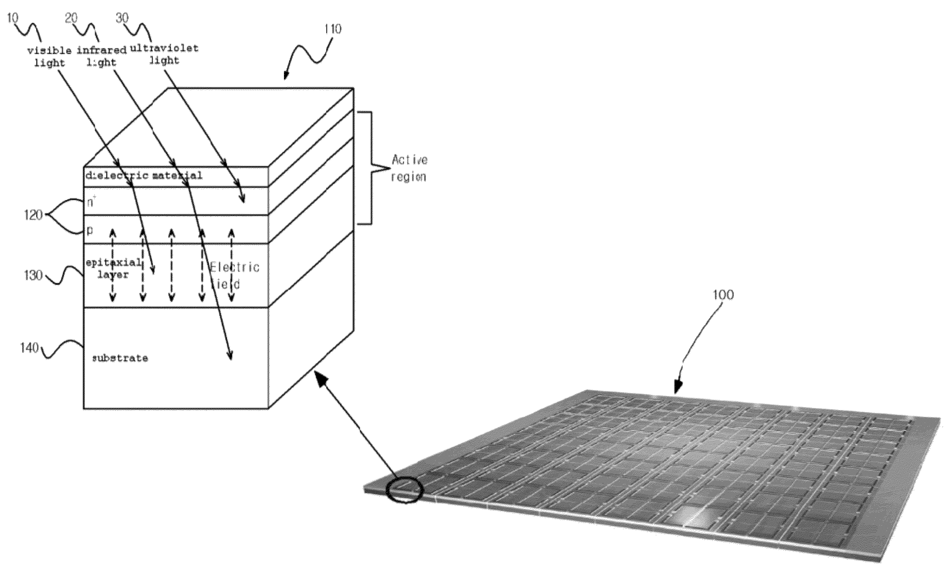
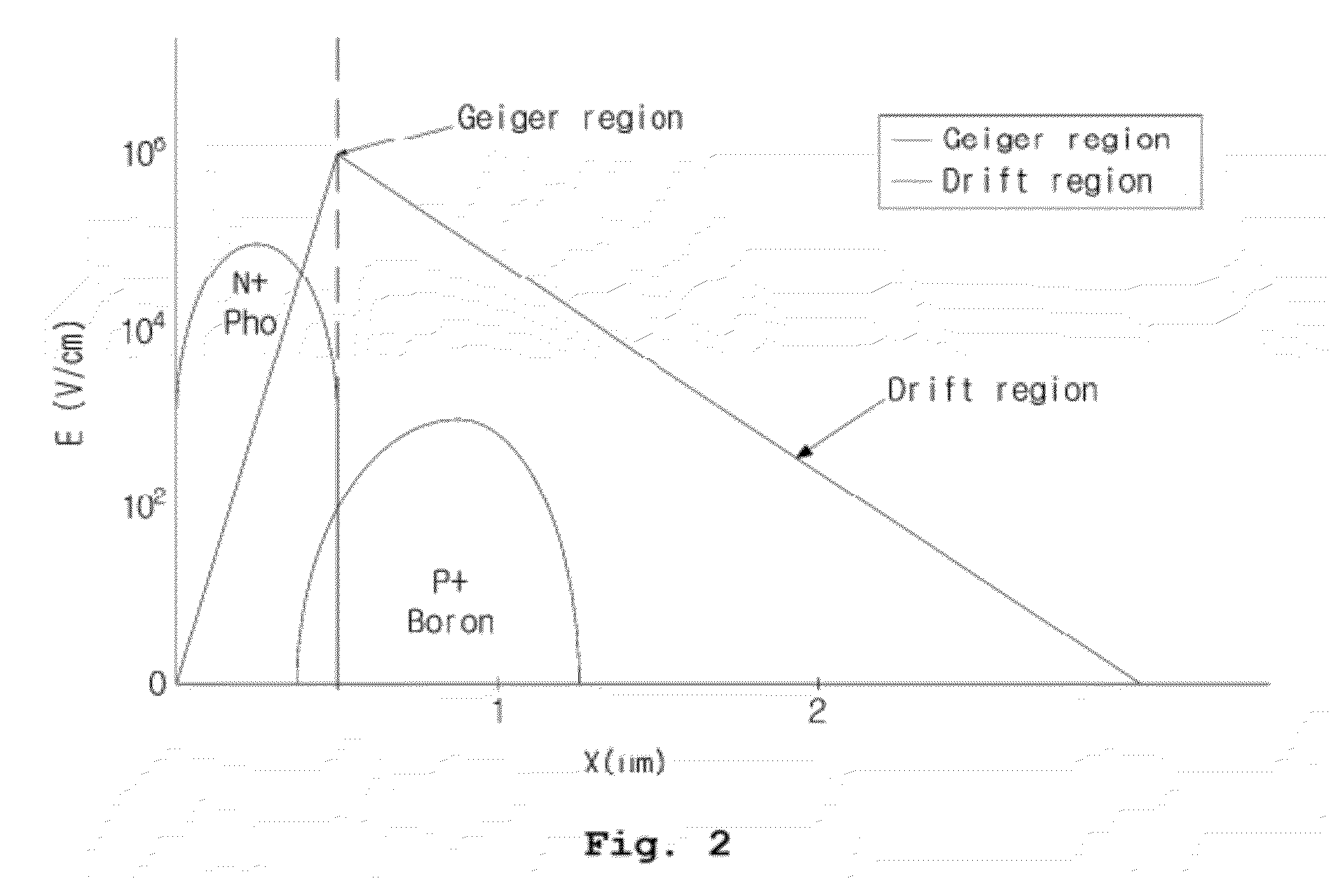
[0007]An aspect of the present invention is to address the above-mentioned problems and / or disadvantages and to provide at least the advantages described below. Accordingly, an aspect of the present invention is to provide a vertical silicon photomultiplier that includes a trench electrode and a PN-junction layer perpendicular to the trench electrode forms and maximizes the quantum efficiency at optical wavelengths, 200˜900 nm in such a way that: it generates electric fields horizontal thereto, by applying a reverse bias voltage between the trench electrode and the PN-junction layer, so that, although ultraviolet light does not reach the PN-junction layer but is incident on the surface, electron-hole pairs can be produced by the horizontally generated electric fields although and an avalanche breakdown can be thus generated; and it allows ultraviolet light, capable of being transmitted in to a relatively deep depth, to react with the PN-junction layer.

Problems solved by technology

On the contrary, silicon photomultipliers (SiPMs) have a disadvantage in that their quantum efficiency is very low, less than 10%, with respect to ultraviolet light of wavelengths 200˜400 nm.
Therefore, the general silicon photomultiplier has low quantum efficiency.

Method used


Image

  • Vertical silicon photomultipler with superior quantum efficiency at optical wavelengths
  • Vertical silicon photomultipler with superior quantum efficiency at optical wavelengths
  • Vertical silicon photomultipler with superior quantum efficiency at optical wavelengths

Examples


Embodiment Construction

[0043]The following description with reference to the accompanying drawings is provided to assist in a comprehensive understanding of exemplary embodiments of the invention as defined by the claims and their equivalents. It includes various specific details to assist in that understanding but these are to be regarded as merely exemplary. Accordingly, those of ordinary skill in the art will recognize that various changes and modifications of the embodiments described herein can be made without departing from the scope and spirit of the invention. In addition, detailed descriptions of well-known functions and constructions may be omitted for clarity and conciseness.

[0044]The terms and words used in the following description and claims are not limited to the bibliographical meanings, but, are merely used by the inventor to enable a clear and consistent understanding of the invention. Accordingly, it should be apparent to those skilled in the art that the following description of exempl...


PUM

PropertyMeasurementUnit
quantum efficiencyaaaaaaaaaa
wavelengthsaaaaaaaaaa
thickaaaaaaaaaa

Abstract

The vertical silicon photomultiplier according to the present invention includes a trench electrode and a PN-junction layer perpendicular to the trench electrode forms and can maximize the quantum efficiency at optical wavelengths, 200˜900 nm in such a way that: it generates electric fields horizontal thereto, by applying a reverse bias voltage to between the trench electrode and the PN junction layer, so that, although ultraviolet light does not reach the PN-junction layer but is incident on the surface, electron-hole pairs can be produced by the horizontally generated electric fields although and an avalanche breakdown can be thus generated, and it allows ultraviolet light, capable of being transmitted to a relatively deep depth, to react with the PN-junction layer.

Description

PRIORITY[0001]This application claims the benefit under 35 U.S.C. §119(a) of a Korean patent application filed on Jan. 29, 2010 in the Korean Intellectual Property Office and assigned Serial No. 10-2010-0008215, the entire disclosure of which is hereby incorporated by reference.BACKGROUND OF THE INVENTION[0002]1. Field of the Invention[0003]The present invention relates to photoelectron systems. More particularly, to a vertical silicon photomultiplier with superior quantum efficiency at optical wavelengths.[0004]2. Description of the Related Art[0005]In recent years, silicon photomultipliers (SiPMs) have developed to replace photomultipliers (PMTs). Silicon photomultipliers (SiPMs) are advantageous in that they are relatively small in size, low in operation voltage, for example, 25˜100 V, and not affected by electric fields, compared with photomultipliers (PMTs). On the contrary, silicon photomultipliers (SiPMs) have a disadvantage in that their quantum efficiency is very low, less ...

Claims


Application Information

Patent Timeline
Patent Type & Authority Applications(United States)
IPC IPC(8): H01L31/0224
CPCG01T1/248H01L27/1446G01T1/241H01L27/14652H01L27/14647B01D47/06B01D53/78B05B1/02
Inventor PARK, IL HUNG
Owner SATBYUL CO LTD
Why Eureka
Try Eureka