

Microelectronic packages with nanoparticle joining
a technology of nanoparticles and microelectronic packages, applied in the direction of semiconductor devices, semiconductor/solid-state device details, electrical apparatus, etc., can solve the problems of difficult to achieve metal columns with uniform height, size and shape, and become more difficult to package semiconductor chips in a flip-chip manner
- Summary
- Abstract
- Description
- Claims
- Application Information
AI Technical Summary
Benefits of technology
Problems solved by technology
Method used
Image

Examples
Embodiment Construction
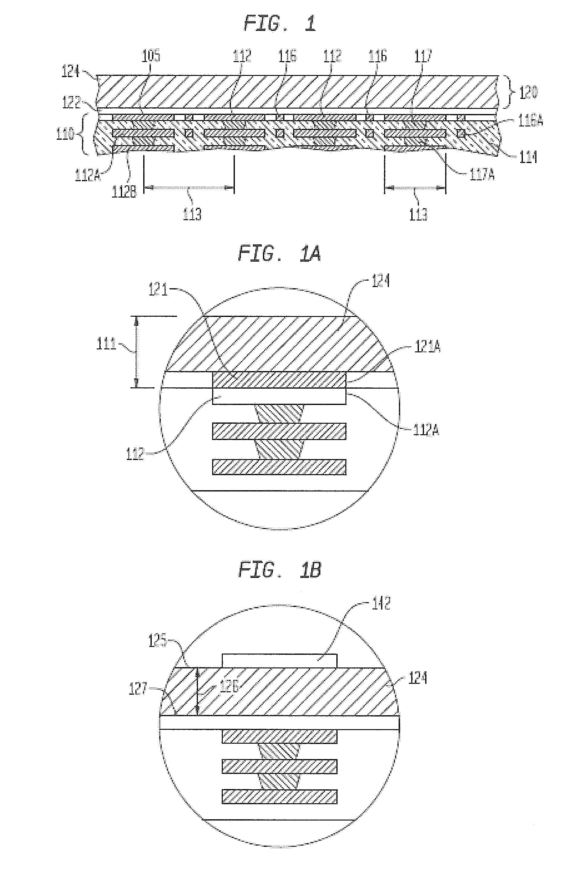
[0060]FIG. 1 is a fragmentary sectional view illustrating a stage in a method of fabricating a substrate having a copper bump interface in accordance with one embodiment herein. As seen in FIG. 1, an interconnection substrate 110, which can be fully or partially formed, is joined with a layered metal structure 120 such that a bond region 122 of the layered metal structure contacts conductive pads 112 exposed at a major surface of a dielectric element or substrate 114. In one particular embodiment, the substrate can include a dielectric element bearing a plurality of conductive elements. In one example, the conductive pads can consist essentially of copper. The conductive elements can include contacts, traces, or both contacts and traces. The contacts can be provided as conductive pads having larger diameters than widths of the traces. Alternatively, the conductive pads can be integral with the traces and can be of approximately the same diameter or only somewhat larger than widths o...
PUM
| Property | Measurement | Unit |
|---|---|---|
| temperature | aaaaa | aaaaa |
| temperature | aaaaa | aaaaa |
| thick | aaaaa | aaaaa |
Abstract
Description
Claims
Application Information