Low Noise VCO Circuit Having Low Noise Bias

a low noise, vco circuit technology, applied in the direction of oscillator, pulse generator, pulse technique, etc., can solve the problems of unstable pll loop, inability of varactor to provide desired capacitance value, etc., and achieve the effect of low noise vco circui

Inactive Publication Date: 2012-02-02
QUINTIC MICROELECTRONICS WUXI
View PDF2 Cites 44 Cited by
  • Summary
  • Abstract
  • Description
  • Claims
  • Application Information

AI Technical Summary

Benefits of technology

[0005]A low noise VCO circuit is disclosed. The low noise LC VCO comprises an LC resonant circuit comprising an inductive element and a pair of capacitive elements, a negative impedance element, and a DC bias circuit. The pair of capacitive elements has a capacitance value controlled by a control voltage. The negative impedance element comprising one or more cross-coupled transistor pairs, wherein each of said one or more cross-coupled transistor pairs comprises a first transistor and a second transistor, wherein first transistor gate is coupled to second transistor drain and second transistor gate is coupled to first transistor drain. The DC bias circuit provides a DC bias to the pair of capacitive elements, wherein the DC bias circuit comprises a current source, a load device and a voltage divider coupled to the load device in parallel. The DC bias is coupled to a middle contact of the voltage divider. The negative impedance element is coupled to the LC resonant circuit to cause the VCO circuit to oscillate at a frequency related to an inductance value of the inductive element and the capacitance value of the capacitive elements. In one embodiment, the load device is selected from a group consist of a PNP transistor, an NPN transistor, a diode-connected NMOS, and a diode-connected PMOS. The voltage divider comprises a first resistor and a second resistor connected in series, wherein a joint contact of the first resistor and the second resistor is coupled to the middle contact. The one or more cross-coupled transistor pairs is selected from a group consisting of a cross-coupled NMOS transistor pair, a cross-coupled PMOS transistor pair, and one cross-coupled NMOS transistor pair and one cross-coupled PMOS transistor pair.

Problems solved by technology

In this case, the varactor may be unable to provide a desired capacitance value according to the linear model of capacitance versus voltage difference.
Consequently, the VCO frequency may deviate from a desired frequency substantially and cause the PLL loop to become unstable.

Method used


Image

  • Low Noise VCO Circuit Having Low Noise Bias
  • Low Noise VCO Circuit Having Low Noise Bias
  • Low Noise VCO Circuit Having Low Noise Bias

Examples


Embodiment Construction

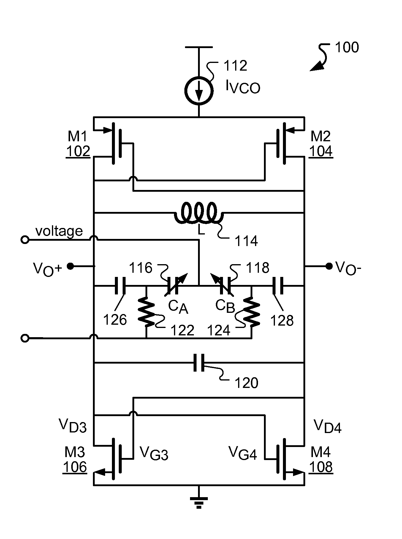
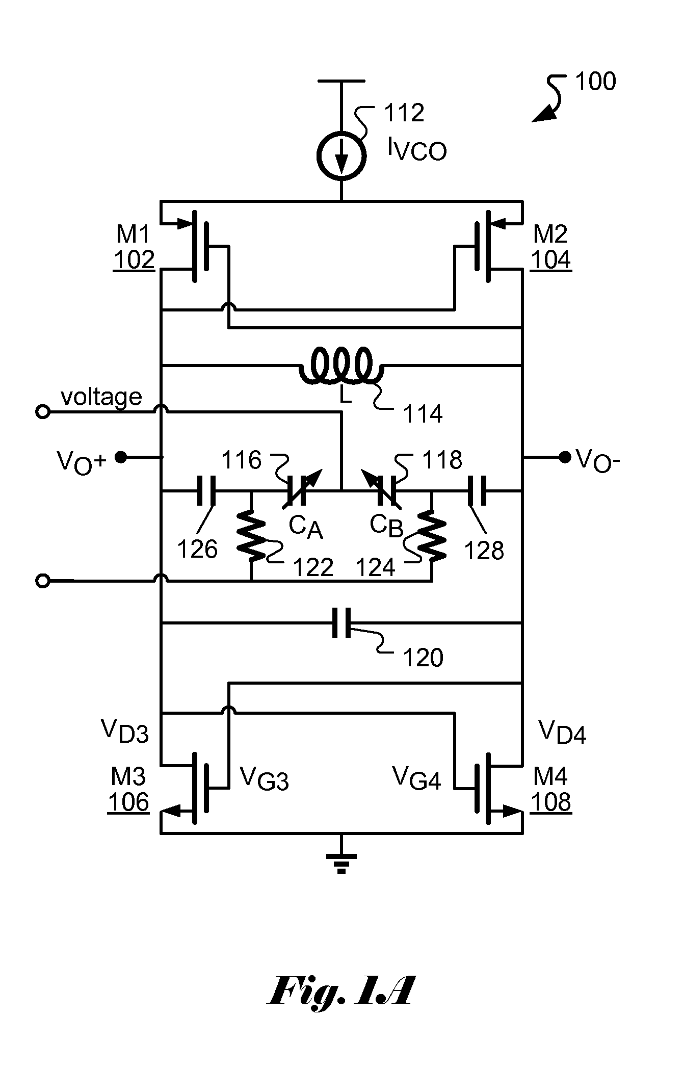
[0017]FIG. 1A illustrates an exemplary VCO circuit 100 incorporating an LC tuning circuit to adjust the frequency, wherein a pair of varactors CA 116 and CB 118 is used for fine frequency tuning. The LC tuning circuit comprises an inductor L 114, a fixed capacitor 120, and a pair of adjustable capacitors CA 116 and CB 118. The adjustable capacitors CA 116 and CB 118 are implemented using varactors. A DC bias is supplied to nodes of capacitors CA 116 and CB 118 through respective resistors 122 and 124 and the control voltage is applied to the common node of the two capacitors. Capacitors 126 and 128 serve as DC blocking capacitors to isolate the DC bias voltage from the output nodes VO+ and VO−. The VCO circuit uses cross-coupled transistors M3106 and M4108 as a negative impedance element to cause the LC tuning circuit to oscillate at a desired frequency. In order to increase the efficiency of the VCO circuit, a pair of cross-coupled complementary transistors M1102 and M2104 may also...


PUM


Abstract

A low noise VCO circuit for an LC VCO circuit comprising MOS varactors is disclosed. The LC VCO circuit usually comprises an LC tuning circuit coupled with a pair of cross-coupled transistors used as a negative impedance element. A pair of varactors is used to provide fine tuning by applying a control voltage to the varactor. Since the varactor is also coupled to the pair of cross-coupled transistor, the process variation and temperature change may affect the bias voltage coupled to the pair of varactors. Therefore, a bias circuit usually is used to alleviate the impact of process variation and temperature change associated with the pair of transistor. Nevertheless, the bias voltage typically is implemented by providing a current flowing through a resistor, wherein the current is generated by a current source. The noise associated with the current source will affect the performance of the VCO circuit. A low noise VCO circuit is disclosed which utilizes a low noise bias circuit. The low noise bias circuit comprises a current source, a load device and a voltage divider wherein the load device is coupled to the voltage divider in parallel. The load device may be implemented using a bipolar transistor or a diode-connected MOS device.

Description

CROSS REFERENCE TO RELATED APPLICATIONS[0001]The present invention claims priority to U.S. Provisional Patent Application, No. 61 / 369,683, filed Jul. 31, 2010, entitled “Low Noise VCO Circuit Having Low Noise Bias.” The U.S. Provisional patent application is hereby incorporated by reference in its entirety.FIELD OF THE INVENTION[0002]The present invention relates to circuit for communication systems. In particular, the present invention relates to an LC VCO circuit having a low-noise bias circuit.BACKGROUND[0003]In a radio receiver, a radio frequency (RF) signal is typically received using an antenna and the received RF is then processed along the receive path to recover the signal transmitted. In the receive path, the received signal is subject to various processing such as amplifying, filtering, down-converting, demodulating, and etc. The input signal usually covers a range of frequencies designated for a particular band. For example, for a terrestrial broadcast TV receiver, the t...

Claims


Application Information

Patent Timeline
Patent Type & Authority Applications(United States)
IPC IPC(8): H03B5/12
CPCH03B2200/0062H03B5/1243H03B5/1212H03B5/1228
Inventor YANG, YULI, XUECHUXUAN, PEIQI
Owner QUINTIC MICROELECTRONICS WUXI
Why Eureka
Try Eureka