Plasma processing apparatus

a plasma processing and inductive coupling technology, applied in the direction of plasma technique, chemical vapor deposition coating, coating, etc., can solve the problems of difficult control of plasma distribution within the chamber as desired, difficult to generate plasma, and difficult to generate plasma

Inactive Publication Date: 2012-02-09
TOKYO ELECTRON LTD
View PDF11 Cites 25 Cited by
  • Summary
  • Abstract
  • Description
  • Claims
  • Application Information

AI Technical Summary

Benefits of technology

[0015]To solve the above-mentioned problems, in accordance with one aspect of the present disclosure, there is provided a plasma processing apparatus including an evacuable processing chamber for performing therein a plasma process on a substrate; a substrate mounting table for mounting thereon the substrate within the processing chamber; a dielectric window provided to face the substrate mounting table via a processing space; a multiple number of high frequency antennas disposed in a space adjacent to the processing space with the dielectric window positioned therebetween; a gas supply unit for supplying a processing gas into the processing space; a high frequency power supply for applying a high frequency power to the multiple number of high frequency antennas to thereby generate plasma of the processing gas by an inductive coupling; and a combination preventing member for preventing induced magnetic fields corresponding to the multiple number of high frequency antennas from being combined with each other.
[0021]Further, the multiple number of high frequency antennas may be spaced apart from each other at a distance enough for preventing the induced magnetic fields corresponding to the multiple number of high frequency antennas from being combined with each other.
[0023]In accordance with the present disclosure, it is possible to generate plasma in one-to-one correspondence to the high frequency antennas according to a high frequency power, and it is also possible to control a plasma distribution within the processing chamber.

Problems solved by technology

In the ICP processing apparatus, however, even if a multiple number of RF antennas are provided and a high frequency power for plasma generation (hereinafter, referred to as an “excitation RFH”) applied to the RF antennas is controlled, it may be difficult to generate plasma so as to be distributed in one-to-one correspondence to the RF antennas.
That is, it may be difficult to control a plasma distribution within the chamber as desired.
That is, in the conventional plasma processing apparatus, it may be difficult to generate plasma in one-to-one correspondence to the RF antennas 203a and 203b.
Thus, it may be difficult to control a plasma distribution within the chamber.

Method used


Image

  • Plasma processing apparatus
  • Plasma processing apparatus
  • Plasma processing apparatus

Examples


first embodiment

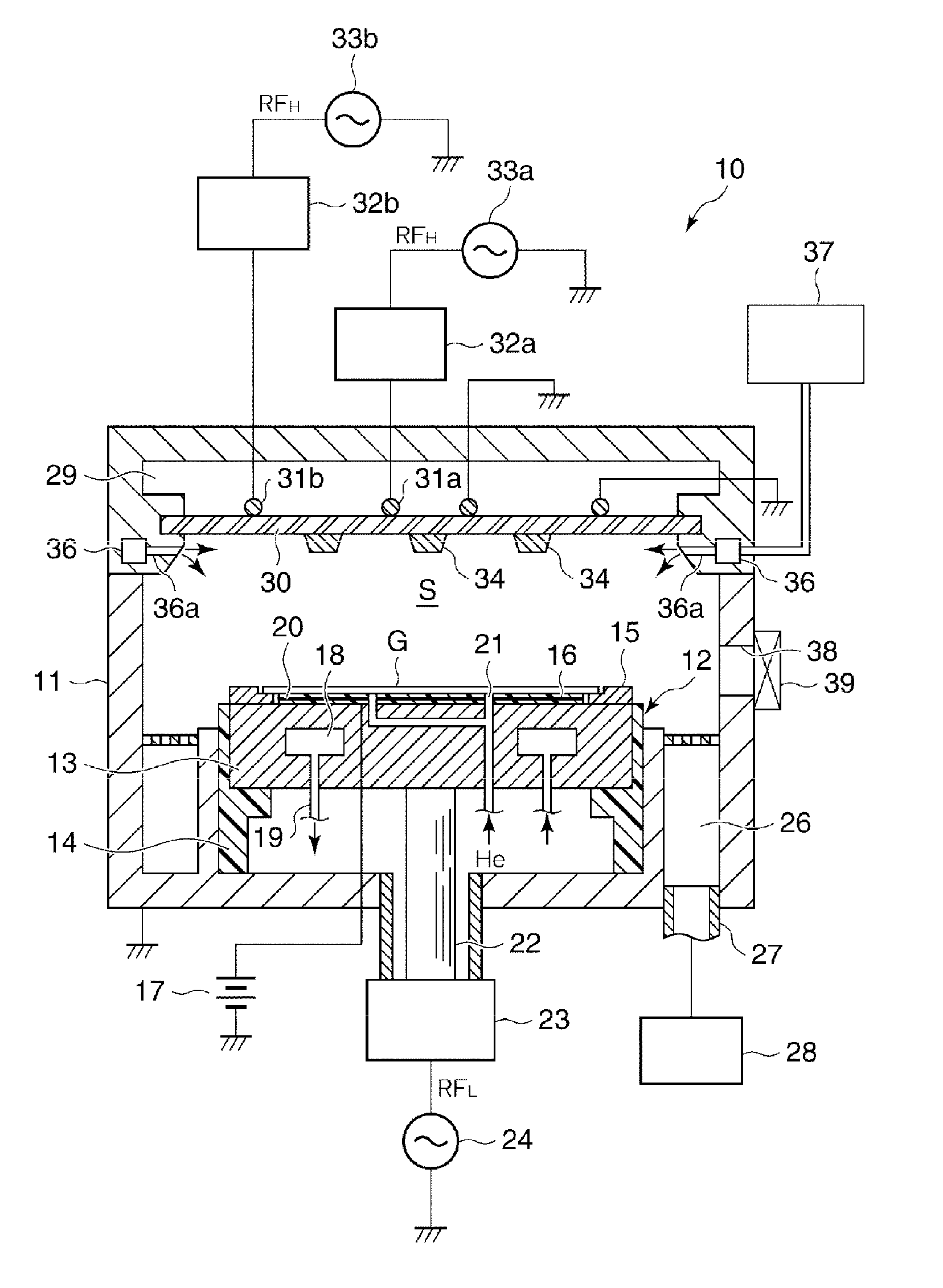
[0042]FIG. 1 is a cross sectional view schematically illustrating a configuration of a plasma processing apparatus in accordance with the present disclosure. This plasma processing apparatus performs a plasma process such as etching process or film forming process on, e.g., a glass substrate for manufacturing a liquid crystal display (LCD).

[0043]As depicted in FIG. 1, a plasma processing apparatus may include a processing chamber 11 for accommodating therein a glass substrate to be processed (hereinafter, simply referred to as a “substrate”) G. A cylindrical mounting table (susceptor) 12 for mounting thereon the substrate G is provided in a lower part of the chamber 11. The susceptor 12 may mainly include a base member 13 made of, e.g., aluminum of which surface is alumite-treated, and the base member 13 is supported on a bottom of the chamber 11 with an insulating member 14 provided therebetween. A top surface of the base member 13 is a substrate mounting surface on which the subst...

second embodiment

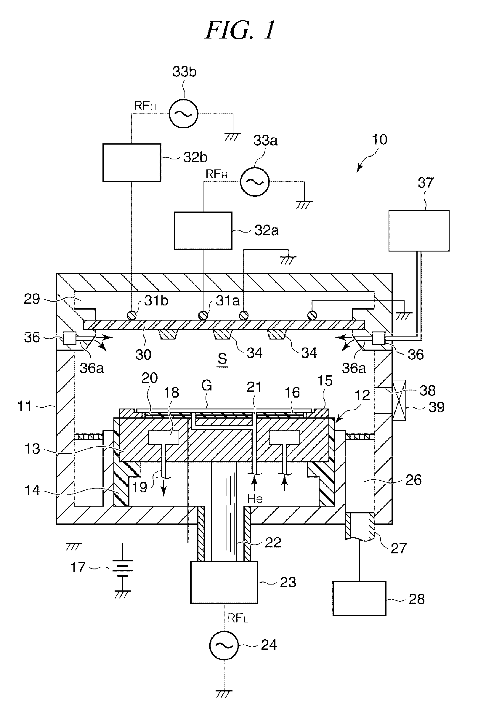
[0062]FIG. 2 is a cross sectional view schematically illustrating a major configuration of a plasma processing apparatus in accordance with the present disclosure.

[0063]Recently, as a size of the substrate G to be processed increases, the chamber 11 is also getting scaled up. Further, in order to maintain a vacuum level in the interior of the chamber 11 having such a big size, a thickness of the dielectric window 30 is also getting larger. If the thickness of the dielectric window 30 becomes larger, a distance between RF antennas 31a and 31b and a processing space S within the chamber 11 is increased, so that a combined magnetic field may be easily formed at an intermediate position between the adjacent RF antennas. As a result, it may be difficult to form plasma in one-to-one correspondence to the respective RF antennas. The second embodiment is designed to solve such a problem. In accordance with the second embodiment, a thickness of a portion of the dielectric window 30 correspon...

third embodiment

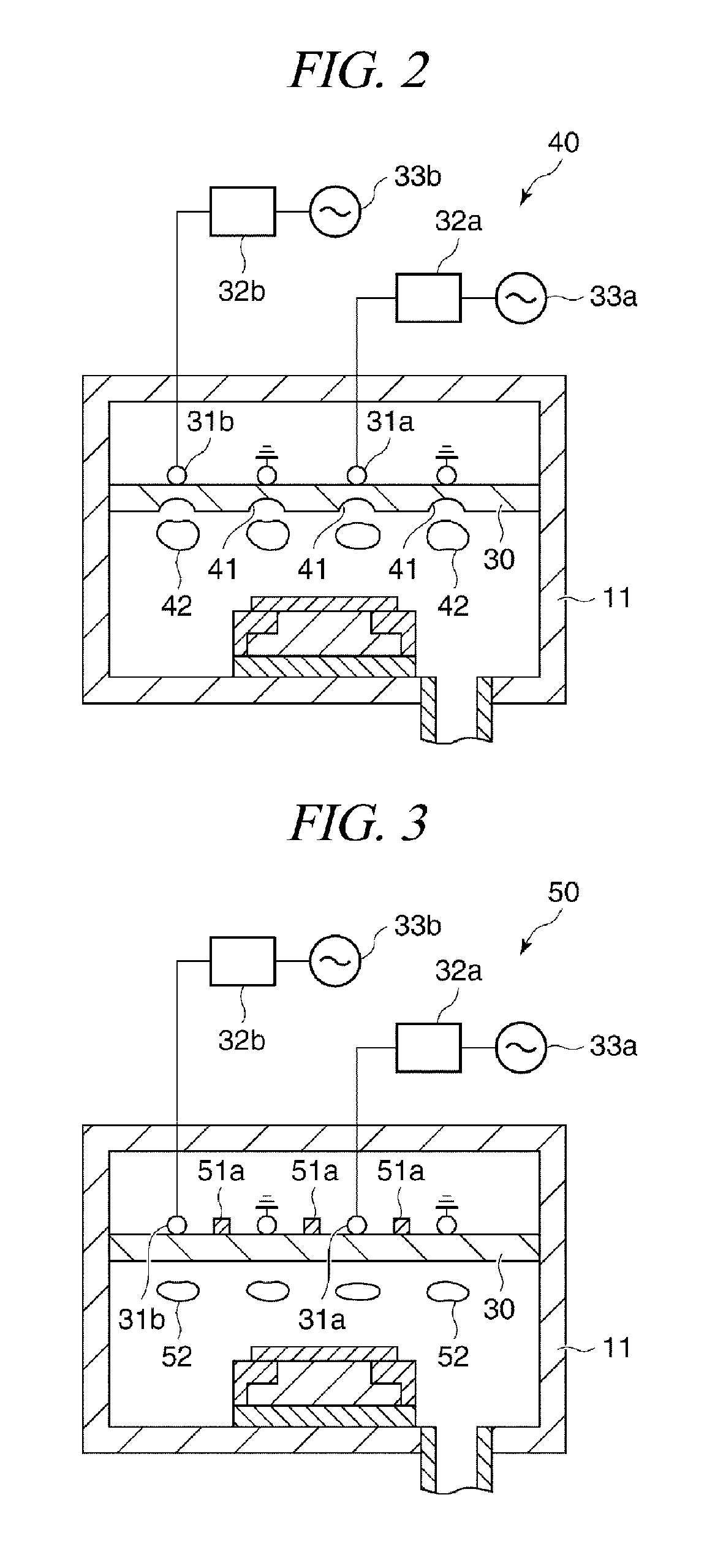
[0068]FIG. 3 is a cross sectional view schematically illustrating a major configuration of a plasma processing apparatus in accordance with the present disclosure.

[0069]As depicted in FIG. 3, a plasma processing apparatus 50 is different from the plasma processing apparatus 10 of FIG. 1 in the following configuration. That is, instead of forming the circular ring-shaped or circular protrusions 34 made of the dielectric material at the positions on the bottom surface of the dielectric window 30 corresponding to the inter-position of the RF antennas 31a and 31b, circular ring-shaped or circular protrusions 51a made of a material having a magnetic permeability different from that of a dielectric window 30 are formed on a top surface of the dielectric window 30 at positions corresponding to the inter-position of the RF antennas 31a and 31b.

[0070]In accordance with the third embodiment, since the circular ring-shaped or circular protrusions 51a made of the material having the magnetic p...


PUM

PropertyMeasurementUnit
internal pressureaaaaaaaaaa
frequencyaaaaaaaaaa
thicknessaaaaaaaaaa

Abstract

A plasma processing apparatus includes: an evacuable chamber 11 for performing therein a plasma process on a substrate G; a susceptor 12 for mounting thereon the substrate G within the chamber 11; a dielectric window 30 provided to face the susceptor 12 via a processing space S; RF antennas 30a and 30b disposed in a space adjacent to the processing space S with the dielectric window 30; a gas supply unit 37 for supplying a processing gas into the processing space S; a high frequency power supply for applying a high frequency RFH to the RF antennas 30a and 30b, and generating plasma of the processing gas within the processing space S by an inductive coupling; and a protrusion 34 made of a dielectric material and provided on a bottom surface of the dielectric window 30 corresponding to an inter-position of the RF antennas 30a and 30b.

Description

CROSS-REFERENCE TO RELATED APPLICATION[0001]This application claims the benefit of Japanese Patent Application No. 2010-175401 filed on Aug. 4, 2010 and U.S. Provisional Application Ser. No. 61 / 375,562 filed on Aug. 20, 2010, the entire disclosures of which are incorporated herein by reference.FIELD OF THE INVENTION[0002]The present disclosure relates to an inductively coupled plasma processing apparatus for performing a plasma process on a substrate.BACKGROUND OF THE INVENTION[0003]In a manufacturing process of a semiconductor device or a flat panel display (FPD) such as a liquid crystal display (LCD), there is known a plasma processing apparatus for performing a plasma process on various kinds of substrates such as a glass substrate. The plasma processing apparatus can be classified into a capacitively coupled plasma processing apparatus and an inductively coupled plasma processing apparatus according to a plasma generation method.[0004]In an inductively coupled plasma processing ...

Claims


Application Information

Patent Timeline
Patent Type & Authority Applications(United States)
IPC IPC(8): H01L21/3065C23C16/50
CPCH01J37/32623H01J37/3211H01L21/3065H05H1/46
Inventor KOSHIMIZU, CHISHIO
Owner TOKYO ELECTRON LTD
Why Eureka
Try Eureka