Method for forming aluminum metal gate

An aluminum metal and gate technology, which is applied in the field of semiconductor manufacturing process, can solve the problems affecting the reliability of semiconductor devices and the resistivity deviation of aluminum metal gates, and achieve the effects of ensuring normal resistivity, improving reliability and avoiding corrosion.

Active Publication Date: 2012-07-04
SEMICON MFG INT (SHANGHAI) CORP +1
View PDF6 Cites 11 Cited by
  • Summary
  • Abstract
  • Description
  • Claims
  • Application Information

AI Technical Summary

Problems solved by technology

This phenomenon directly leads to the deviation of the resistivity of the aluminum metal gate, which affects the reliability of semiconductor devices.

Method used


Image

  • Method for forming aluminum metal gate
  • Method for forming aluminum metal gate
  • Method for forming aluminum metal gate

Examples


no. 1 example

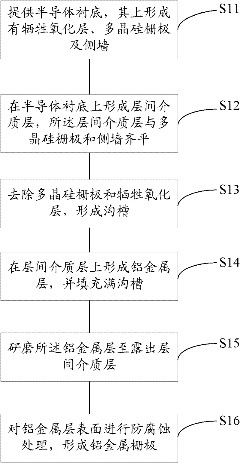
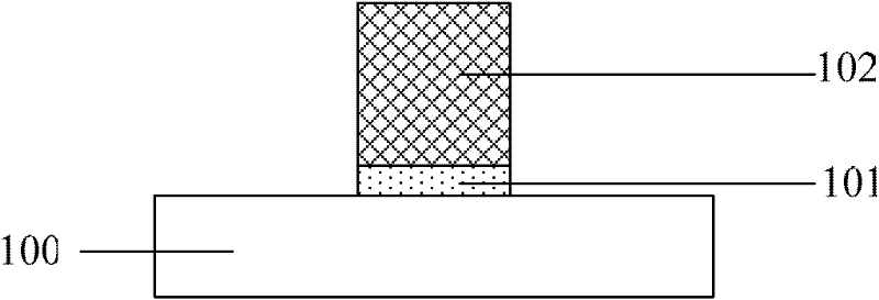
[0043] Figure 2 to Figure 4 It is a schematic diagram of the first specific embodiment of the method for forming an aluminum metal gate provided by the present invention. Such as figure 2 As shown, a semiconductor substrate 100 is provided; a sacrificial oxide layer 101 and a polysilicon gate 102 are sequentially formed on the semiconductor substrate 100. A sacrificial oxide layer 101 is formed on the sacrificial oxide layer; a polysilicon layer is formed on the sacrificial oxide layer 101; a first photoresist layer (not shown) is formed on the polysilicon layer, and a grid pattern is defined after exposure and development; The first photoresist layer is a mask, and the polysilicon layer and the sacrificial oxide layer 102 are etched along the gate pattern to expose the semiconductor substrate 100 to form the polysilicon gate 102 .

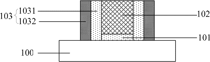
[0044] Such as image 3As shown, side walls 103 are formed on the semiconductor substrate 100 on both sides of the polysilicon gate 102; Th...

no. 2 example

[0055] Figure 8 to Figure 14 It is a schematic diagram of a second specific embodiment of the method for forming an aluminum metal gate of the present invention. Such as Figure 8 As shown, a semiconductor substrate 200 is provided; a sacrificial oxide layer 201 and a polysilicon gate 202 are sequentially formed on the semiconductor substrate 200 , and the specific process for forming the polysilicon gate 202 is as described in the first embodiment.

[0056] Such as Figure 9 As shown, sidewalls 203 are formed on the semiconductor substrate 200 on both sides of the polysilicon gate 202; the sidewalls 203 include a silicon oxide layer 2031 and a silicon nitride layer 2032 located on both sides of the polysilicon. Example.

[0057] Such as Figure 10 As shown, an interlayer dielectric layer 204 is formed on a semiconductor substrate 200; the surface of the interlayer dielectric layer 204 is flush with the tops of the polysilicon gate 202 and the sidewall 203, and the specif...


PUM


Abstract

The invention relates to a method for forming an aluminum metal gate. The method comprises the following steps of: providing a semiconductor substrate, wherein a sacrificial oxide layer, a dummy gate and spacers are formed on the semiconductor substrate in turn, the spacers are positioned on the semiconductor substrate on the two sides of the dummy gate, and interlayer dielectric (ILD) layers are formed on the semiconductor substrate on the two sides of the dummy gate and on the two sides of each spacer and flush with the dummy gate and the spacers; removing the dummy gate and the sacrificial oxide layer to form a groove; forming an aluminum metal layer on the ILD layers, and filling the groove; grinding the aluminum metal layer until the ILD layers are exposed; and performing anti-corrosion treatment on the surface of the aluminum metal layer to form the aluminum metal gate. By the method for forming the aluminum metal gate, the surface of the aluminum metal gate can be prevented from being corroded, so that the resistivity of the aluminum metal gate is ensured, and the electrical property and reliability of a semiconductor device are improved.

Description

technical field [0001] The invention relates to a semiconductor manufacturing process, in particular to a method for forming an aluminum metal gate. Background technique [0002] With the improvement of integration in integrated circuits, the feature size of the semiconductor manufacturing process is getting smaller and smaller, and the traditional polysilicon gates are gradually replaced by metal gates due to their electrical performance defects. At present, in the technology of 32 nanometers and below, the gate structure basically uses a high-k dielectric as the gate dielectric layer, and a metal layer as the gate to meet the requirements of the electrical performance of the device. [0003] The existing process for preparing metal gates is generally to first prepare a polysilicon gate structure with a traditional process, form a source / drain in the semiconductor substrate, and form an interlayer dielectric on the semiconductor substrate that is flush with the surface of t...

Claims


Application Information

Patent Timeline
Patent Type & Authority Applications(China)
IPC IPC(8): H01L21/28
Inventor 蒋莉黎铭琦
Owner SEMICON MFG INT (SHANGHAI) CORP
Why Eureka
Try Eureka