Light-emitting device having enhanced luminescence by using surface plasmon resonance and method of fabricating the same

a surface plasmon resonance and light-emitting device technology, applied in the direction of semiconductor devices, basic electric elements, electrical devices, etc., can solve the problems of insufficient efficiency and brightness of the qd light-emitting device to be applied to a display, and the life of the organic light-emitting material of the oled is relatively short, so as to achieve the effect of enhancing luminescen

Active Publication Date: 2012-02-09
SAMSUNG ELECTRONICS CO LTD
View PDF3 Cites 51 Cited by
  • Summary
  • Abstract
  • Description
  • Claims
  • Application Information

AI Technical Summary

Benefits of technology

[0008]Provided is an organic light-emitting device (“OLED”) having enhanced luminescence by using surface plasmon resonance.

Problems solved by technology

However, a lifetime of an organic light-emitting material of the OLED is relatively short, and a complicated and expensive film forming process is necessary.
However, in spite of the aforementioned merits, efficiency and brightness of the QD light-emitting device are not sufficient to be applied to a display.

Method used


Image

  • Light-emitting device having enhanced luminescence by using surface plasmon resonance and method of fabricating the same
  • Light-emitting device having enhanced luminescence by using surface plasmon resonance and method of fabricating the same
  • Light-emitting device having enhanced luminescence by using surface plasmon resonance and method of fabricating the same

Examples


Embodiment Construction

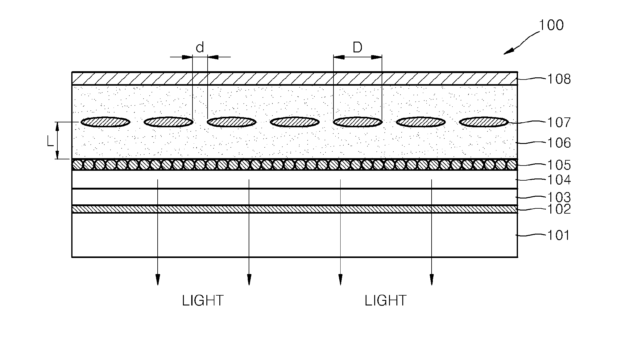
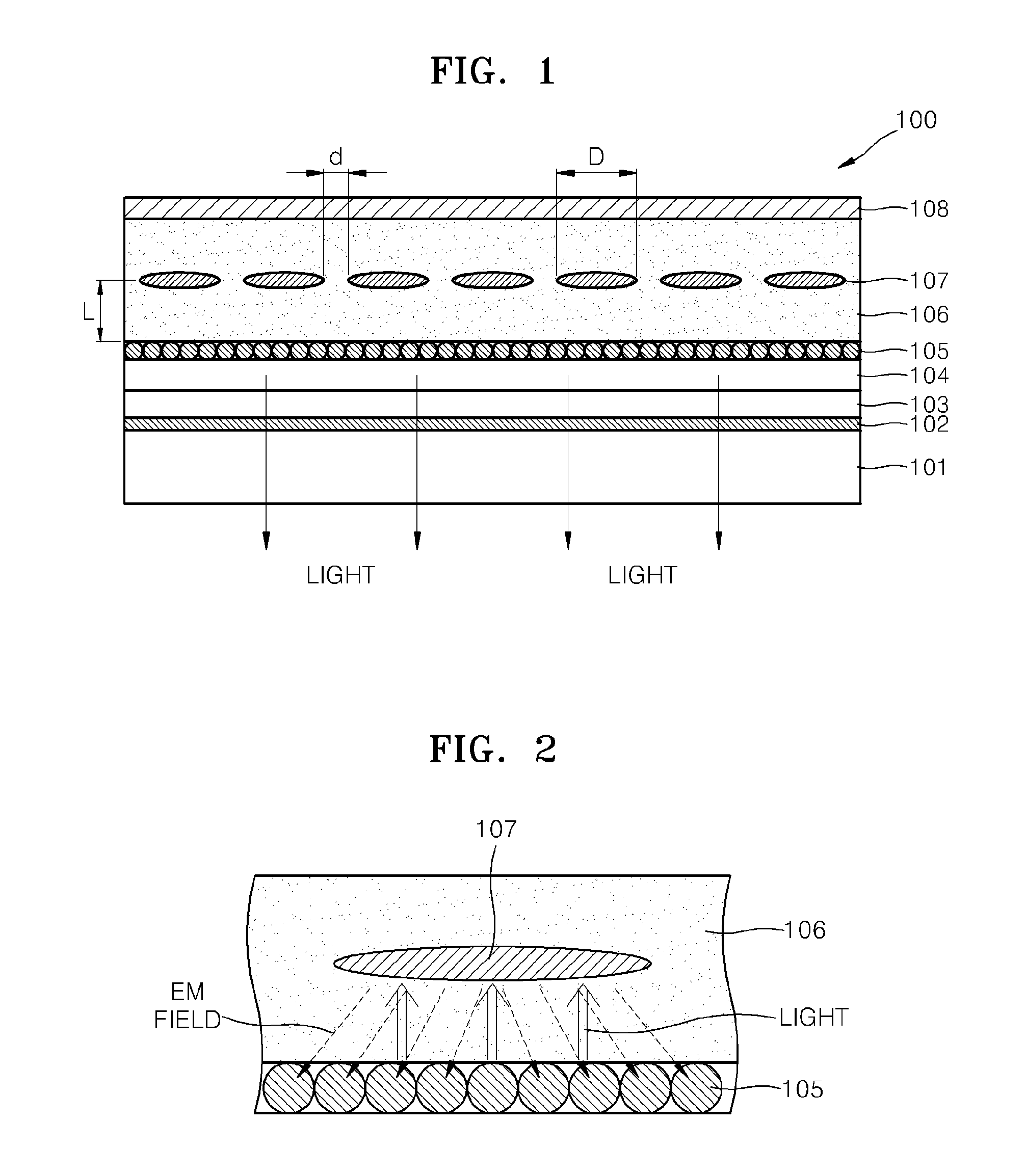
[0044]Reference will now be made in detail to embodiments, examples of which are illustrated in the accompanying drawings, wherein like reference numerals refer to like elements throughout and the size of each component may be exaggerated for clarity. In this regard, the present embodiments may have different forms and should not be construed as being limited to the descriptions set forth herein. Accordingly, the embodiments are merely described below, by referring to the figures, to explain aspects of the present description.

[0045]It will be understood that when an element or layer is referred to as being “on” another element or layer, the element or layer can be directly on another element or layer or intervening elements or layers. In contrast, when an element is referred to as being “directly on” another element or layer, there are no intervening elements or layers present. As used herein, connected may refer to elements being physically and / or electrically connected to each oth...


PUM


Abstract

A quantum dot light-emitting device includes a substrate, a first electrode, a hole injection layer (“HIL”), a hole transport layer (“HTL”), an emitting layer, an electron transport layer (“ETL”), a plurality of nanoplasmonic particles buried in the ETL, and a second electrode.

Description

CROSS-REFERENCE TO RELATED APPLICATIONS[0001]This application claims priority to Korean Patent Application No. 10-2010-0075983, filed on Aug. 6, 2010, and all the benefits accruing therefrom under §119, the disclosure of which is incorporated herein in its entirety by reference.BACKGROUND[0002]1. Field[0003]Provided is a quantum dot (“QD”) light-emitting device or an organic light-emitting device (“OLED”), and method of fabricating the same, and more particularly, to a QD light-emitting device or an OLED having enhanced luminescence by using surface plasmon resonance and method of fabricating the same.[0004]2. Description of the Related Art[0005]An organic light-emitting device (“OLED”) uses a thin film formed of an organic material as an emitting layer. The OLED may be formed of various types of materials, such as a high-purity thin film. However, a lifetime of an organic light-emitting material of the OLED is relatively short, and a complicated and expensive film forming process i...

Claims


Application Information

Patent Timeline
Patent Type & Authority Applications(United States)
IPC IPC(8): H01L51/52H01L51/56
CPCH01L27/3211H01L51/5262H01L51/5048H01L51/502H10K59/35H10K50/115H10K50/14H10K50/85H10K50/00
Inventor KIM, TAE-HOLEE, CHANG-WONCHOI, BYOUNG-LYONGCHO, KYUNG-SANG
Owner SAMSUNG ELECTRONICS CO LTD
Why Eureka
Try Eureka