

Semiconductor device and method for fabricating the same
a technology of semiconductor devices and semiconductor devices, applied in the direction of basic electric elements, chemical vapor deposition coatings, coatings, etc., can solve the problems of poor uniform thickness of barrier-metal films on the bottom of contact holes, poor electrical characteristics of semiconductor devices, etc., to achieve accurate control of the shape of contact holes, low fabrication costs, and increased width of contact holes
- Summary
- Abstract
- Description
- Claims
- Application Information
AI Technical Summary
Benefits of technology
Problems solved by technology
Method used
Image

Examples
Embodiment Construction
[0028]Embodiments of the invention will now be described with reference to the attached drawings, in which like elements are indicated by like reference characters.
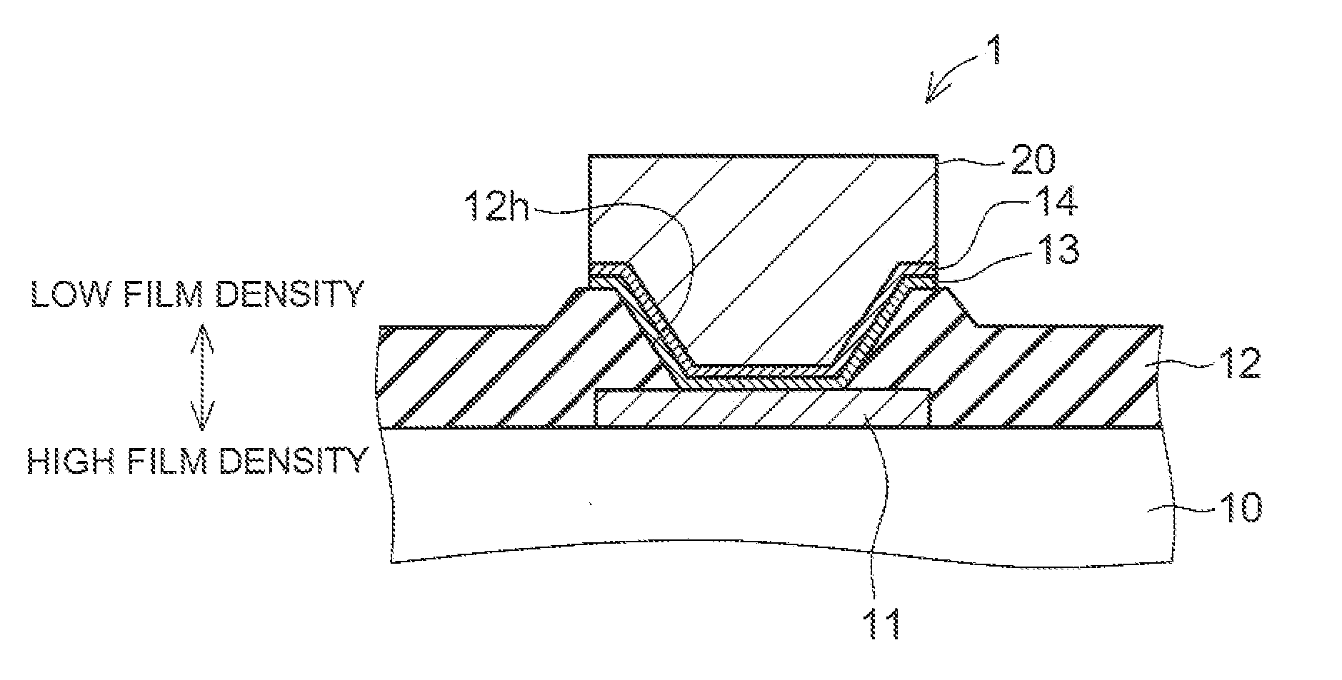
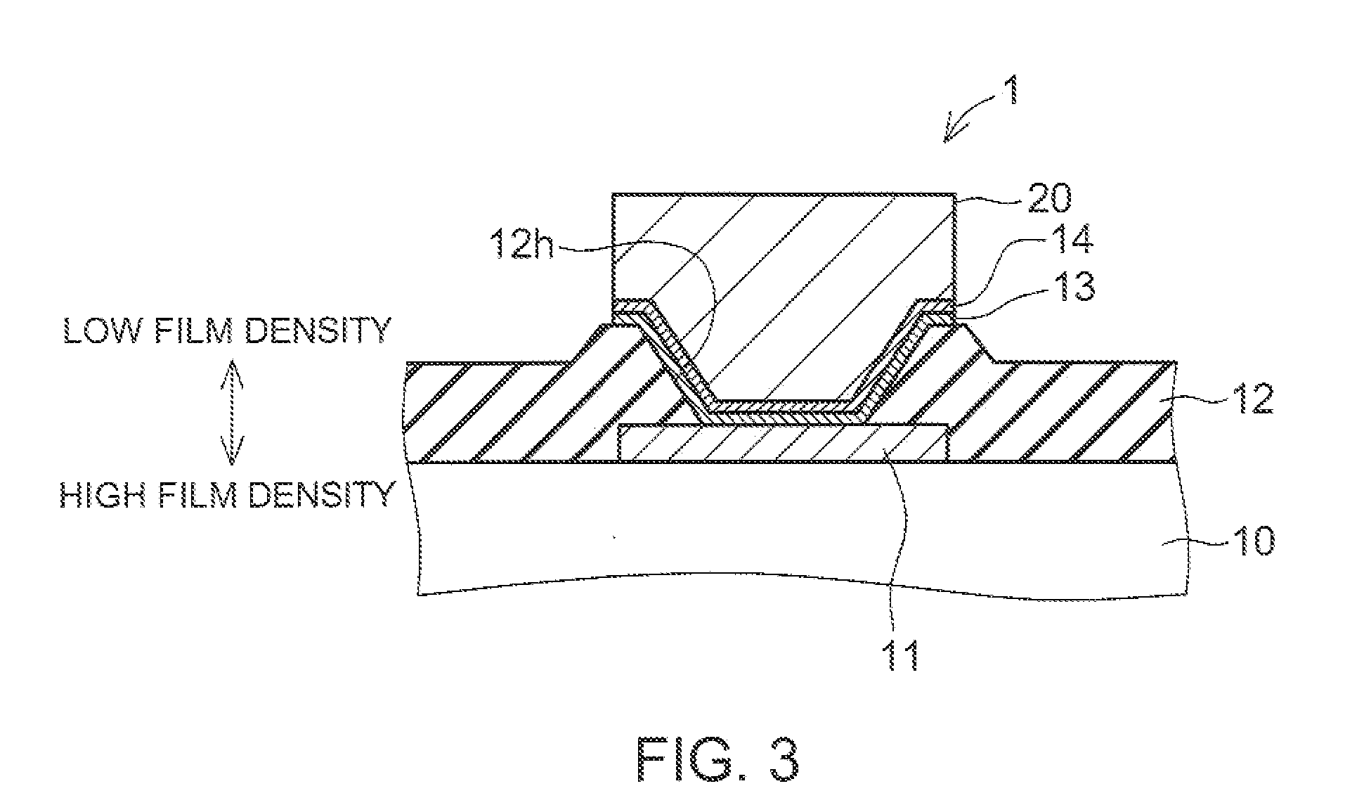
[0029]FIG. 3 is a schematic cross-sectional view of a semiconductor device 1 or an embodiment. The semiconductor device 1 includes a semiconductor substrate 10, a passivation film 12, a lower electrode (i.e., an electrode pad) 11, UBM layers (under-bump metal layers or underlying metal layers) 13, 14 and a bump electrode (i.e., an upper electrode) 20. The semiconductor substrate 10 is used as a base substrate on which a layered structure is formed. The lower electrode 11 is formed on the main surface of the semiconductor substrate 10, and the passivation film 12 is formed over the main surface of the semiconductor substrate 10. The UBM layers 13, 14 are formed on both the lower electrode 11 and the hole wall 12h of the passivation film 12. The bump electrode 20 is formed on the UBM layer 14. On the main surface of the sem...
PUM
| Property | Measurement | Unit |
|---|---|---|
| Thickness | aaaaa | aaaaa |
| Power | aaaaa | aaaaa |
| Density | aaaaa | aaaaa |
Abstract
Description
Claims
Application Information