Semiconductor device driving unit and method

a technology of semiconductor devices and driving units, which is applied in the direction of oscillator generators, pulse techniques, electronic switching, etc., can solve the problems of increasing the loss of igbt and fwd during the transition period at the time of switching, and the surge voltage occurs during the transition period, so as to suppress the increase of switching loss and reduce the surge voltage

Active Publication Date: 2012-02-09
HONDA MOTOR CO LTD
View PDF3 Cites 13 Cited by
  • Summary
  • Abstract
  • Description
  • Claims
  • Application Information

AI Technical Summary

Benefits of technology

[0025]One or more embodiments of the invention provide a unit and a method for driving a semiconductor device having a switching function, which are capable of reducing a surge voltage while suppressing an increase in switching loss at a time of switching of the semiconductor device.

Problems solved by technology

However, a surge voltage occurs during the transition period at the time of switching such as the turning on or off of the IGBT.
However, in the case of the electric vehicle inverter, it is difficult to ensure such installation space in electric vehicles, so that it is extremely difficult to adopt a large-size IGBT.
However, if the switching speed is reduced to reduce the surge voltage, the loss of the IGBT and FWD during the transition period at the time of switching (hereinafter, referred to as “switching loss”) is increased in turn.
However, it is difficult to say that these conventional methods sufficiently satisfy the demand.

Method used


Image

  • Semiconductor device driving unit and method
  • Semiconductor device driving unit and method
  • Semiconductor device driving unit and method

Examples


Embodiment Construction

[0037]Hereinafter, an embodiment of the present invention will be described with reference to the drawings.

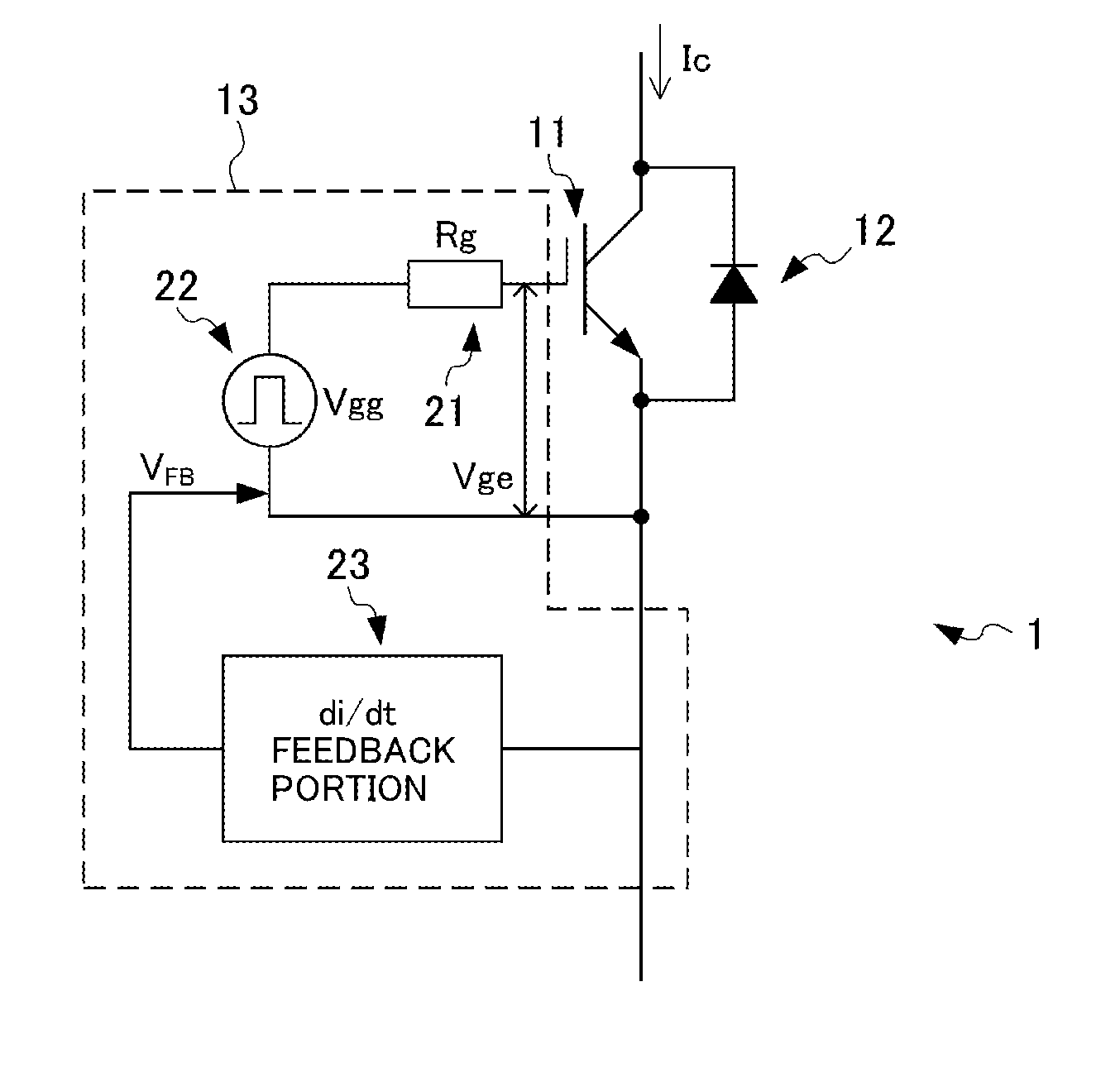
[0038]FIG. 1 is a view showing the schematic structure of the embodiment of an electronic circuit 1 including a semiconductor device driving circuit 13.

[0039]The electronic circuit 1 is adoptable, for example, as part of a power module of the electric vehicle inverter. The electronic circuit 1 is provided with an IGBT 11, an FWD 12 and the semiconductor device driving circuit 13.

[0040]The IGBT 11 and the FWD 12 are connected in parallel to each other in such a way that the input and output directions thereof are opposite to each other.

[0041]The IGBT 11 has a switching function of connecting and shutting off the bus such as the power line of the inverter, and is turned on or off according to the magnitude of the voltage of the driving signal supplied to the gate of the IGBT 11, that is, according to the magnitude of the gate-emitter voltage Vge. The semiconductor device driving ...


PUM


Abstract

A semiconductor device (11) having a switching function of being turned on or off according to a voltage (Vge) of a driving signal supplied to a gate thereof is driven by generating a feedback voltage (VFE) based on a time change (dI/dt) of a collector current (Ic) of the semiconductor device (11) and applying the feedback voltage (VFE) as part of the voltage (Vge) of the driving signal when the semiconductor device (11) is switched from on to off.

Description

BACKGROUND OF THE INVENTION[0001]1. Field of the Invention[0002]The present invention relates to a unit and a method for driving a semiconductor device having a switching function. Specifically, the present invention relates to a unit and a method for driving a semiconductor device, capable of reducing a surge voltage while suppressing an increase in switching loss at the time of switching of the semiconductor device.[0003]2. Related Art[0004]Conventionally, in an electric vehicle, a synchronous electric motor driven by three-phase alternating current is typically used. Thus, the electric vehicle is provided with an inverter that converts the direct-current output from a battery (direct-current power source) into three-phase alternating current to drive the synchronous electric motor. The inverter provided in the electric vehicle will particularly be referred to as “electric vehicle inverter”.[0005]Many electric vehicle inverters adopt PWM (pulse width modulation) control, and adopt...

Claims


Application Information

Patent Timeline
Patent Type & Authority Applications(United States)
IPC IPC(8): H02J1/00
CPCH03K17/0828H03K17/168H03K17/166
Inventor TSUKADA, YOSHINARI
Owner HONDA MOTOR CO LTD
Why Eureka
Try Eureka