Solid-state imaging device and electronic camera

Inactive Publication Date: 2012-02-09
PANASONIC CORP
View PDF2 Cites 53 Cited by
  • Summary
  • Abstract
  • Description
  • Claims
  • Application Information

AI Technical Summary

Benefits of technology

[0032]According to the present invention, the highly-accurate AF can be achieve

Problems solved by technology

However, the above-mentioned conventional high-pixel-density digital still cameras have the following problems.
Therefore, the volume of the digital still camera is increased, requiring high cost.
Moreover, in the method disclosed in Patent Reference 2, the amou

Method used


Image

  • Solid-state imaging device and electronic camera
  • Solid-state imaging device and electronic camera
  • Solid-state imaging device and electronic camera

Examples


Example

Embodiment 1

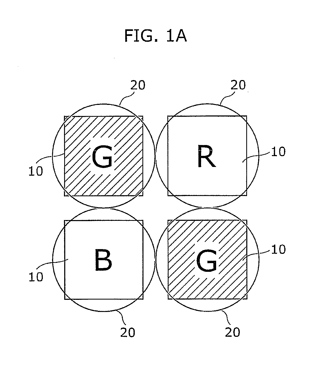
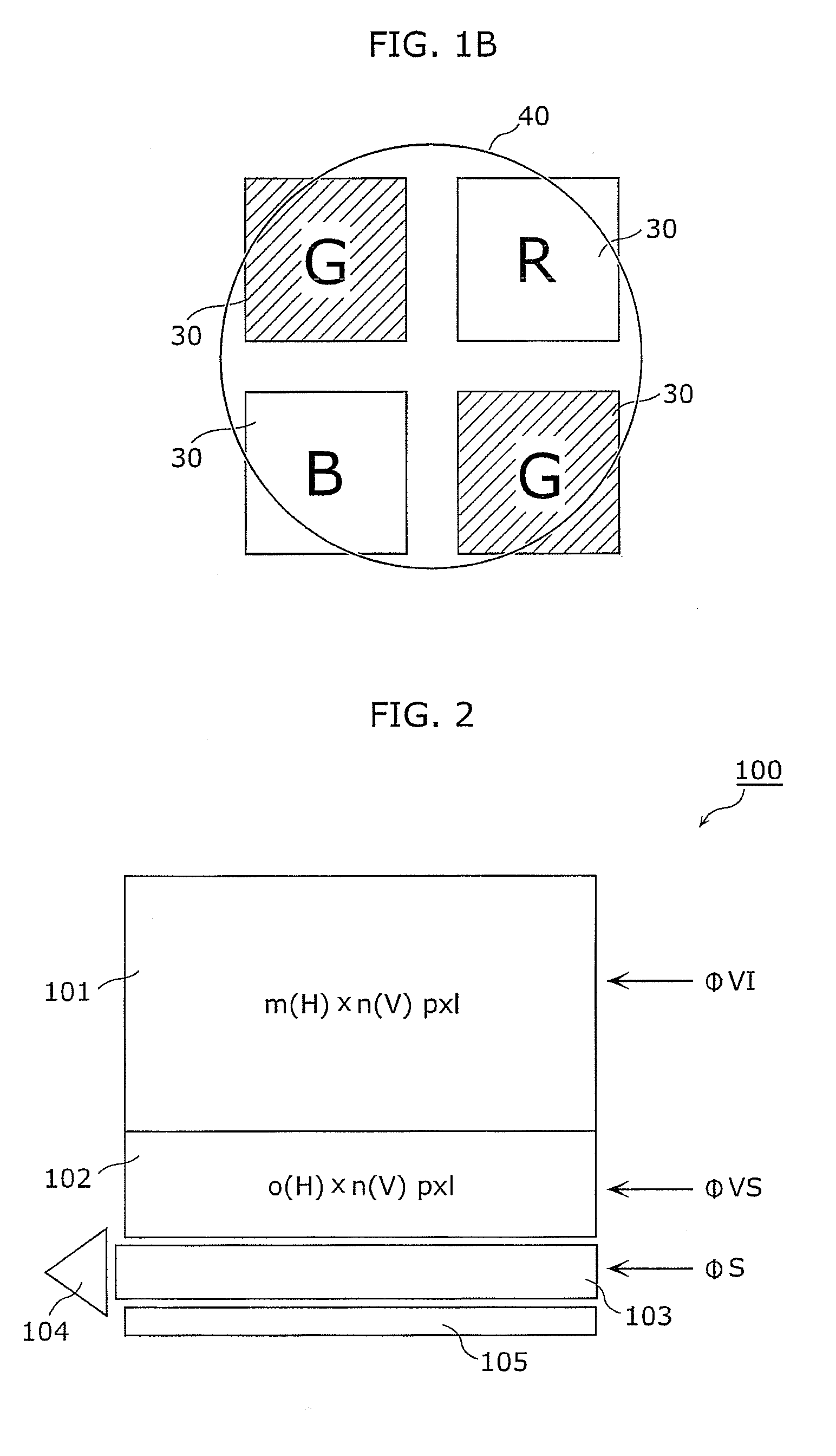
[0063]The solid-state imaging device according to Embodiment 1 includes a plurality of photoelectric conversion units configured to convert incident light to an electronic signal and arranged in a two dimensional array. The photoelectric conversion units are divided into a group of normal pixels having microlenses arranged to correspond in a one-to-one relationship and a group of AF pixels having microlenses arranged to correspond in a many-to-one relationship. In other words, a single microlens is disposed to each set of a predetermined number, which is two or more, of photoelectric conversion units of the photoelectric conversion units included in the AF pixel group.

[0064]First, a basic pixel arrangement in the solid-state imaging device according to this embodiment is described with reference to FIGS. 1A and 1B. FIG. 1A illustrates an example of an arrangement of photoelectric conversion units 10 and microlenses 20 of the normal pixel group. FIG. 1B illustrates an exa...

Example

Embodiment 2

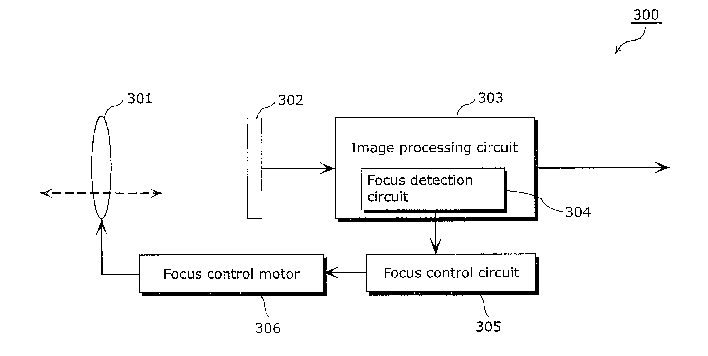
[0138]The electronic camera according to this embodiment is an electronic camera having an AF function and including the solid-state imaging device described in Embodiment 1.

[0139]Note that the electronic camera according to this embodiment may be a movie camera having a function of capturing moving pictures, an electronic still camera having a function of capturing still image, and other cameras such as an endoscope and a monitoring camera. These cameras are essentially the same.

[0140]FIG. 20 is a schematic view showing a configuration of an electronic camera 300 according to this embodiment. The electronic camera 300 shown in FIG. 20 includes an image capturing lens 301, a solid-state imaging element 302, an image processing circuit 303, a focus detection circuit 304, a focus control circuit 305, and a focus control motor 306.

[0141]The incident light entering through the imaging lens 301 (focus lens) forms an image on the solid-state imaging element 302. The solid-stat...


PUM


Abstract

An object of the present invention is to provide a highly-accurate AF without adding a mechanism of the camera or increasing the power consumption. A solid-state imaging device according to an aspect of the present invention includes: a plurality of photoelectric conversion units configured to convert incident light into electronic signals, the photoelectric conversion units being arranged in a two dimensional array, the photoelectric conversion units including a plurality of first photoelectric conversion units and a plurality of second photoelectric conversion units; a plurality of first microlenses each of which is disposed to cover a corresponding one of said first photoelectric conversion units; and a second microlens disposed to cover the second photoelectric conversion units, in which at least two of the second photoelectric conversion units are located at respective positions which are offset from an optical axis of the second microlens, in mutually different directions.

Description

CROSS REFERENCE TO RELATED APPLICATION[0001]This is a continuation application of PCT application No. PCT / JP2010 / 001180 filed on Feb. 23, 2010, designating the United States of America.BACKGROUND OF THE INVENTION[0002](1) Field of the Invention[0003]The present invention relates to solid-state imaging devices and electronic cameras, and particularly relates to a solid-state imaging device and an electronic camera having an auto focus (AF) function.[0004](2) Description of the Related Art[0005]Recently, applications for handling images by a computer have been significantly increased. Particularly, a digital camera for taking images into a computer has been extensively commercialized. The development of such a digital camera, especially a digital still camera handling still images, shows clear tendency of increased number of pixels.[0006]For example, the number of pixels of an imaging element of a camera for moving pictures (video movie) is generally 250,000 to 400,000, while a camera...

Claims


Application Information

Patent Timeline
IPC IPC(8): H04N5/335G02B7/34G03B13/36H04N5/232H04N5/372H04N9/07H04N101/00
CPCH04N5/23212H04N5/3696H04N2201/0084H04N9/07H04N9/045H01L27/14621H01L27/14627H01L27/14623H04N23/672H04N25/704H04N23/12H04N25/134
Inventor NAKAMURA, KENJIUEDAMIYAZAKI, KYOICHI
Owner PANASONIC CORP
Why Eureka
Try Eureka