Method of manufacturing multilayer printed wiring board and multilayer wiring board obtained thereby

a manufacturing method and technology of multi-layer printed wiring boards, applied in the direction of printed circuit manufacturing, printed circuit aspects, non-conductive materials with dispersed conductive materials, etc., can solve the problems of increasing the thickness of copper layers on the surface, reducing the thickness of films, and reducing the thickness of thicknesses, etc., to achieve superior conductivity and long-term stability, reduce thickness, and yield higher

Active Publication Date: 2012-02-16
TATSUTA ELECTRICWIRE & CABLE
View PDF2 Cites 3 Cited by
  • Summary
  • Abstract
  • Description
  • Claims
  • Application Information

AI Technical Summary

Benefits of technology

[0009]In view of such circumstances as described above, it is an object of the present invention to provide a manufacturing method in which a multilayer printed wiring board (hereinafter, referred to as “multilayer board”) superior in conductivity and long-term stability even when a general pre-prep, which is advantageous in terms of cost, is used, and a multilayer board obtained thereby.
[0016]The multilayer board obtained by a method of manufacturing according to the present invention allows fine line patterning because a cap plating is not used, thereby satisfying the demand of reduction in thickness. Also, since the metal powders contained in the conductive paste are alloyed and the metal powder and end surfaces of the conductive layer in through holes are alloyed, so that superior conductivity and long-term stability are achieved. Also, since the problem of spreading or the like does not occur, a general pre-preg can be used, which is advantageous in terms of cost. Also, formation of a stacked via structure is possible. Furthermore, a super-multilayer board can be manufactured with higher yield by joining the multilayer board and the multilayer board. As described above, a high-quality multilayer board in which various problems of the related art are solved can be provided using a general apparatus at low cost.

Problems solved by technology

Multi-layering is inevitable in miniaturization of the printed wiring board and, in order to achieve the multi-layering, reduction of thickness is a technical challenge.
However, the former has a probability of extension of the board after having polished the paste and hence the reduction of the thickness of the film is limited, while the cap plating results in increase in thickness of the copper layers on the surfaces which causes a difficulty of fine patterning.
In contrast, the latter has problems of an inability to provide a via hole on a via hole (stacked via), insufficient smoothness of the surface of the board, and generation of cracks at the time of a long-term reliability test.
However, utilization of such paste causes a problem of generation of roughness because the board immediately above the paste is swelled under normal pressing conditions, and also causes a problem of insufficient long-term reliability because the change rate of conductivity over time is high.
However, when forming a through hole with the alloying paste described above, it is necessary to slow down a curing speed of the paste resin component because alloying is hindered if the paste resin component is completely cured before a low melting metal is melted.
However, a general pre-preg has problems in that if the curing speed of the paste resin component is slowed down, the conductive paste may spread at the time of pressing, and the resin component of the pre-preg and the paste may be mixed, thereby failing to obtain desired characteristics.

Method used


Image

  • Method of manufacturing multilayer printed wiring board and multilayer wiring board obtained thereby
  • Method of manufacturing multilayer printed wiring board and multilayer wiring board obtained thereby
  • Method of manufacturing multilayer printed wiring board and multilayer wiring board obtained thereby

Examples


Embodiment Construction

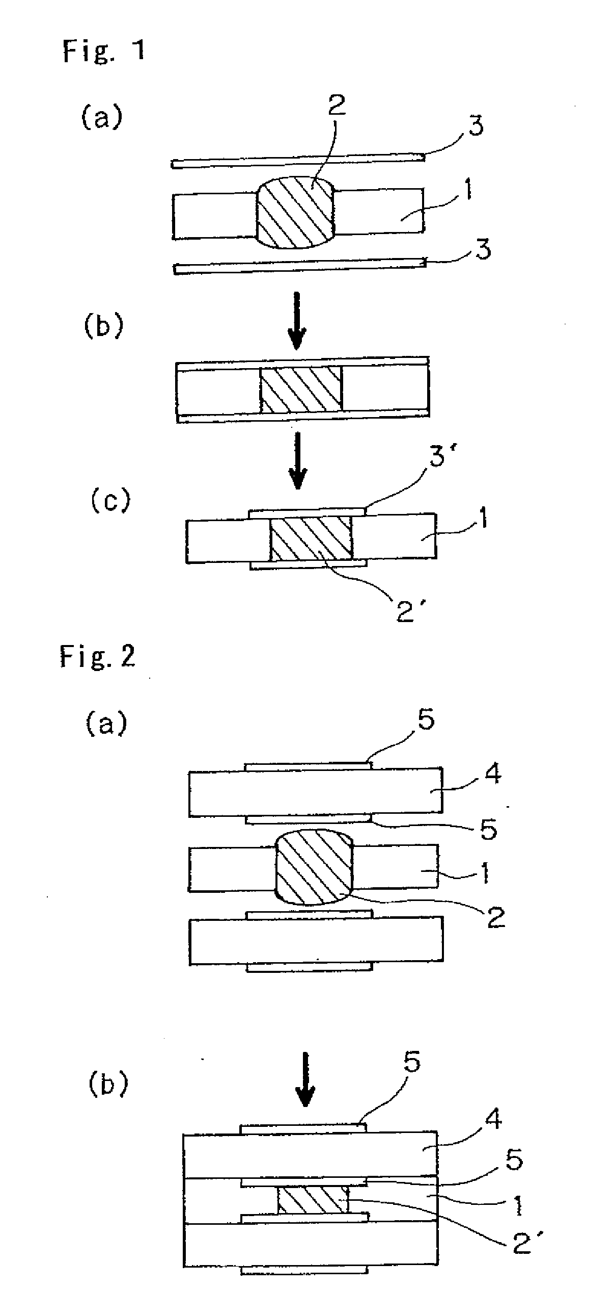
[0023]A method of manufacturing a multilayer board according to the present invention includes at least (1) a process of preheating before providing via holes through a pre-preg, (2) a process of providing the via holes through the preheated pre-preg by laser beam machining, (3) a process of filling conductive paste in the via holes, (4) a process of arranging copper layers or copper layer portions of patterned boards on upper and lower surfaces of the filled conductive paste and pressing for unifying the same. In the process (3) described above, alloying paste containing metal powders melted by being heated at the time of curing of the paste wherein melted metal powders are alloyed with respect to each other is used as the conductive paste. In the process (4), if the copper layers which are not patterned are laminated, the patterning is performed after the pressing.

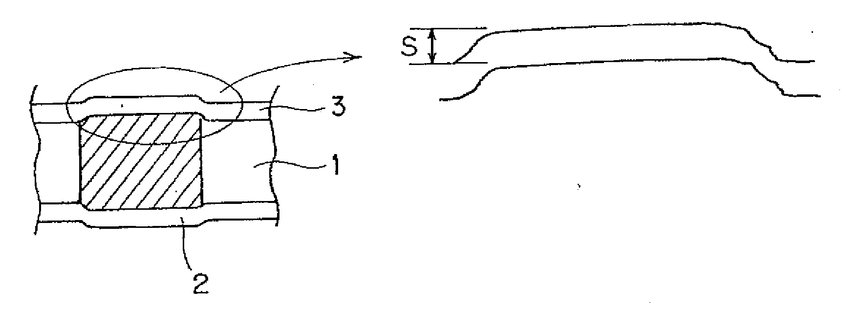
[0024]Referring now to the drawings, description of the present invention will be given further in detail. FIG. 1 show...


PUM

PropertyMeasurementUnit
temperatureaaaaaaaaaa
melting pointaaaaaaaaaa

Abstract

In a method of manufacturing a multilayer board, including: a drilling step for forming a via hole through a pre-preg by laser beam machining, a step of filling the via hole with conductive paste containing a resin component and metal powder, and a step of arranging copper layers or copper layer portions of patterned boards on and under the filled conductive paste and pressing the same, a multilayer printed wiring board superior in conductivity and long-term stability is obtained by using alloying paste as the conductive paste in which at least part of the metal powder is melted and the metal powders adjacent to each other are alloyed, using a pre-preg having a ratio A / B of at least 10 before subjected to preheating, where A is a storage modulus at an inflection point where the storage modulus changes from increasing to decreasing and B is a storage modulus at an inflection point where the storage modulus changes from decreasing to increasing in a temperature profile rising from 60° C. to 200° C., and preheating the pre-preg before the drilling step to reduce the ratio A / B to below 10.

Description

BACKGROUND OF THE INVENTION[0001]The present invention relates to a method of manufacturing a multilayer wiring board and a multilayer wiring board obtained thereby and, more specifically, a method of manufacturing a multilayer wiring board in which via holes are filled with conductive paste containing metal powder.[0002]In recent years, in association with a trend toward reduction of thickness and length of products in the field of electronics, the similar needs are increasing also for a printed wiring board. Multi-layering is inevitable in miniaturization of the printed wiring board and, in order to achieve the multi-layering, reduction of thickness is a technical challenge.[0003]As a method of manufacturing the multilayer wiring board of the related art, there is a method including (a) providing a via hole on a core board 10 having copper layer layers 11 on both surfaces of an insulated material, applying a through hole plating 12 on a wall surface of the via hole and then printi...

Claims


Application Information

Patent Timeline
Patent Type & Authority Applications(United States)
IPC IPC(8): H05K1/09H05K3/30
CPCH01B1/22H05K2203/1194H05K3/0032H05K3/4069H05K3/462H05K2201/0272H05K2201/0355H05K2201/10378H05K2203/0425H05K2203/1461H05K1/0298H05K3/46Y10T29/49124Y10T29/49165Y10T29/49155Y10T29/49139Y10T29/49117H05K2201/0191H05K2203/0278H05K2203/1105H05K2203/111H05K2203/1572H05K1/095H05K1/09
Inventor YAMAGUCHI, NORIHIROUMEDA, HIROAKIYUKAWA, KEN
Owner TATSUTA ELECTRICWIRE & CABLE
Why Eureka
Try Eureka