Trench mosfet with integrated schottky rectifier in same cell

a technology of mosfet and rectifier, which is applied in the direction of semiconductor devices, diodes, electrical apparatus, etc., can solve problems such as hazardous problems for semiconductor power devices

Inactive Publication Date: 2012-02-16
FORCE MOS TECH CO LTD
View PDF6 Cites 58 Cited by
  • Summary
  • Abstract
  • Description
  • Claims
  • Application Information

AI Technical Summary

Benefits of technology

[0006]It is therefore an aspect of the present invention to provide a new and improved semiconductor power device such as a trench MOSFET integrated with a Schottky rectifier in same cell by forming a tilt-angle implanted drift region...

Problems solved by technology

If only reducing epitaxial layer resistivity for reducing the parasitic resistance RSGT, the breakdown voltage of the semiconductor power device may not...

Method used


Image

  • Trench mosfet with integrated schottky rectifier in same cell
  • Trench mosfet with integrated schottky rectifier in same cell
  • Trench mosfet with integrated schottky rectifier in same cell

Examples


Embodiment Construction

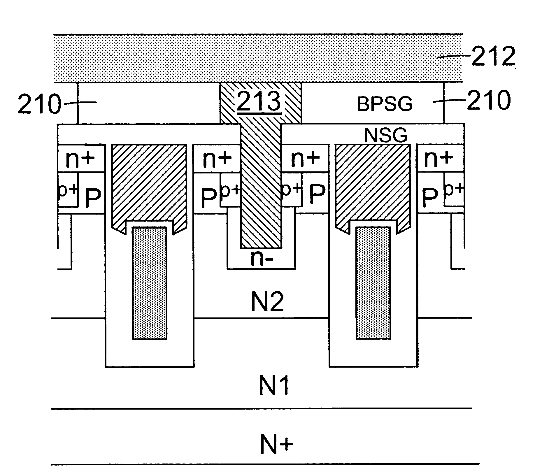
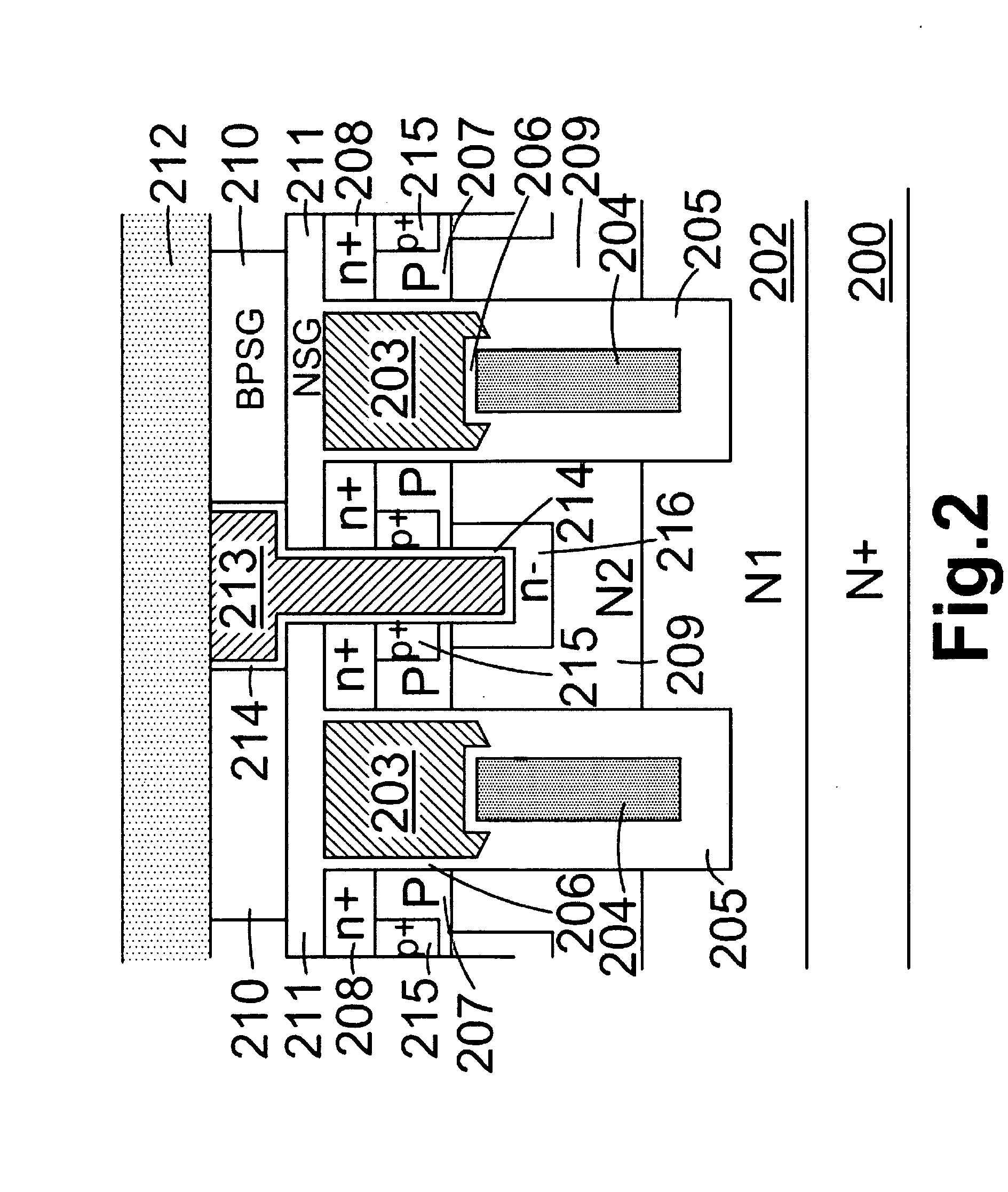
[0020]Please refer to FIG. 2 for cross-sectional view of a trench MOSFET integrated with a Schottky rectifier in same cell according to the present invention where an N-channel trench MOSFET is formed on an N+ substrate 200 supporting an N-epitaxial layer 202 with doping concentration N1. A plurality of trenched gates are formed within said N-epitaxial layer 202 and each of these trenched gates includes a top gate segment 203 and a bottom shielded gate segment 204. The bottom shielded gate segment 204 is padded by a thicker gate oxide layer 205 and the top gate segment is padded by a normal gate oxide layer 206 which is thinner than the thicker gate oxide layer 205. Meanwhile, the bottom shielded gate segment 204 is insulated from the top gate segment 203 by portion of the normal gate oxide layer 206 covering top surface of the thicker gate oxide layer 205 and the bottom shielded gate segment 204. A plurality of P-body regions 207 are formed within the N-epitaxial layer 202 and surr...


PUM


Abstract

A semiconductor power device comprising a plurality of trench MOSFETs integrated with Schottky rectifier in same cell is disclosed. The invented semiconductor power device comprises a tilt-angle implanted drift region having higher doping concentration than epitaxial layer to reduce Vf in Schottky rectifier portion and to reduce Rds in trench MOSFET portion while maintaining a higher breakdown voltage by implementation of thick gate oxide in trench bottom of trenched gates. Furthermore, the invented semiconductor power device further comprises a Schottky barrier height enhancement region to enhance the barrier layer covered in trench bottom of trenched source-body-Schottky contact in Schottky rectifier portion.

Description

FIELD OF THE INVENTION[0001]This invention relates generally to the device configuration and manufacturing methods for fabricating the semiconductor power devices. More particularly, this invention relates to an improved and novel device configuration and manufacturing process for providing trench MOSFET integrated with Schottky rectifier in same cell to improve performance of both MOSFET and Schottky rectifier without degrading breakdown voltage.BACKGROUND OF THE INVENTION[0002]In order to achieve higher switching speed and efficiency for semiconductor power device, a Schottky rectifier is normally added in parallel to the semiconductor power device with a parasitic PN body diode to function as a clamping diode to prevent the body diode of the semiconductor power device from turning on. The Schottky rectifier is single carrier, i.e., electron carrier only and that can be drawn simply by the drain electrode. The requirement for the clamping effect is that the forward voltage Vf of t...

Claims


Application Information

Patent Timeline
IPC IPC(8): H01L29/78H01L21/336
CPCH01L21/26586H01L27/0629H01L29/4236H01L29/7827H01L29/7813H01L29/7806H01L29/7811H01L29/407H01L29/0878H01L29/42376H01L29/1095H01L29/66734H01L29/66727
Inventor HSHIEH, FWU-IUAN
Owner FORCE MOS TECH CO LTD
Why Eureka
Try Eureka