Electro-optical logic techniques and circuits

a logic circuit and optical logic technology, applied in logic circuits, pulse techniques, instruments, etc., can solve problems such as the failure of previous attempts to devise optical logic, the expected stumbling block, and the complexity of copper interconnects becoming more and more complex

Inactive Publication Date: 2012-02-16
THE BOARD OF TRUSTEES OF THE UNIV OF ILLINOIS
View PDF3 Cites 7 Cited by
  • Summary
  • Abstract
  • Description
  • Claims
  • Application Information

AI Technical Summary

Benefits of technology

[0007]The advent of the light-emitting transistor and transistor laser allows the integration of the transistor and laser as a single component or device, adding a natural photonic component to integrated circuits. The light-emitting transistor and transistor laser, due to its direct-gap (III-V semiconductor) structure, possesses a major advantage over its purely electrical cousin: it has the capability of processing (receive, transform and transmit) both electrical and optical signals. For example, besides performing its usual electrical signal processing functions, a light-emitting transistor can convey its output signal via either an electrical output or, where desired, it can propagate the output signals in the form of an optical signal, thereby allowing near lossless, high-speed optical signal transmission (e.g. in optical waveguides) over distances unreachable by copper interconnects.

Problems solved by technology

As computing grows increasingly more complex and performance goals escalate with the implementation of multi-core strategies and massively parallel computing, building blocks are needed that can perform at higher speeds, continue to scale with integrable components to achieve economies of scale, and satisfy the demand for interconnect speeds between each computing component and blocks of transistors.
As the demand for lower power consumption (e.g., longer battery life) increases, copper interconnects are becoming more and more complex, and are expected to hit a stumbling block as increasing peripheral power (e.g., that consumed in pre-amplifier circuitry) will no longer meet the requirements for better performance at lower power.
However, prior attempts at devising optical logic have encountered serious limitations.
Both solutions have major disadvantages that could not be overcome.
The major issue with a laser-photothyristor implementation is that the PNPN-thyristor has an extremely slow switching speed, typically in the MHz range.
This fundamental limitation is owing to the saturated nature of PNPN switch operation.
Once turned on, the PNPN device accumulates large quantities of charges in its base, and can take a long time just to turn off again.
This sets a fundamental limit to the speed of the laser-photothyristor solution.
Regarding a proposed all optical logic gate based on a laser-phototransistor, a key issue is that the solution requires a complex layer structure comprising layers of crystal growth to form a laser on top of a phototransistor, or vice versa.
This results in very complex device fabrication.
The manufacturing process has low yields and low repeatability, negating the possibility for very large scale integration.

Method used


Image

  • Electro-optical logic techniques and circuits
  • Electro-optical logic techniques and circuits
  • Electro-optical logic techniques and circuits

Examples


Embodiment Construction

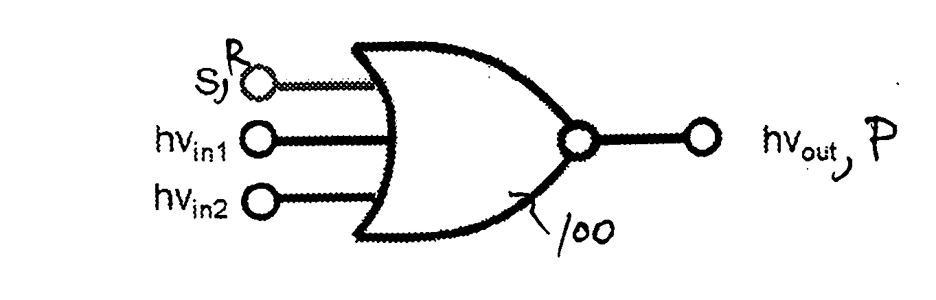
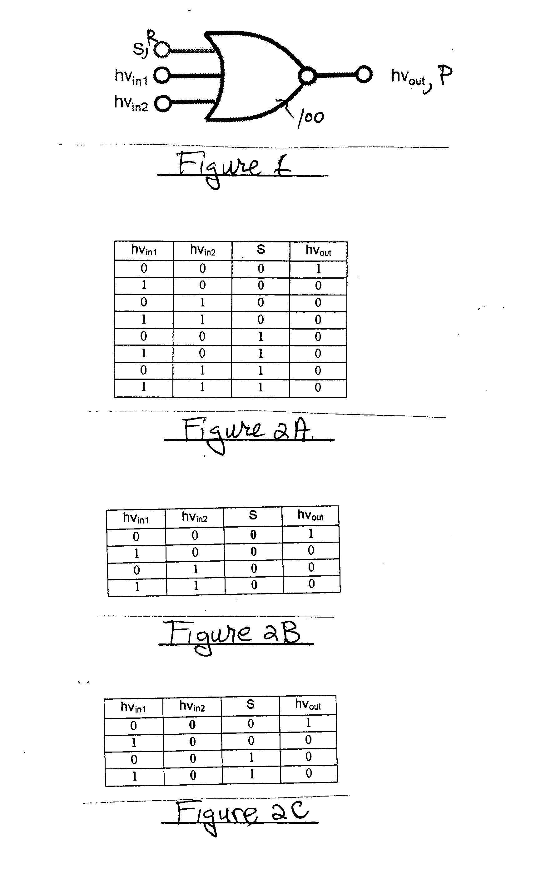
[0030]FIG. 1 illustrates the operation of an embodiment of a universal electro-optical NOR gate 100 which receives two or more signals as inputs. As seen in FIG. 1, the signals can be in the form of optical signals, hvin1 and hvin2, or electrical signals, S, R. It then performs a logic operation, NOR, on the input signals (see logic table of FIG. 2A), and produces its result in the form of an output signal that could be either optical, hvout or electrical, P. For example, if the NOR gate receives no input signal (i.e., all inputs “0”), it will produce an output signal (“1”). If there is a signal detected at the input (i.e., any input is a “1”), the NOR gate will turn off its output signal, hence outputting a logic “0”.

[0031]FIG. 2A shows the logic table for the case of two optical inputs, one electrical input, and an optical output. The table has eight rows representing the eight possible combinations of three binary inputs (23). FIG. 2B shows the logic table for the case of two opt...


PUM

PropertyMeasurementUnit
currentaaaaaaaaaa
opticalaaaaaaaaaa
voltageaaaaaaaaaa

Abstract

A method for implementing an electro-optical logic function responsive to first and second logical inputs, includes the following steps: providing, as an output stage, a light-emitting transistor having an electrical input port and an optical output port; and providing, as an input stage, a circuit for receiving the first and second logical inputs and producing a control signal that is coupled with the electrical input port of the output stage.

Description

PRIORITY CLAIM[0001]Priority is claimed from U.S. Provisional Patent Application Ser. No. 61 / 401,501, filed Aug. 13, 2010, and said U.S. Provisional Patent Application is incorporated herein by reference.FIELD OF THE INVENTION[0002]This invention relates to the field of electro-optical logic circuits and techniques and, more particularly, to such circuits and techniques that employ light-emitting transistors and / or transistor lasers.BACKGROUND OF THE INVENTION[0003]As computing grows increasingly more complex and performance goals escalate with the implementation of multi-core strategies and massively parallel computing, building blocks are needed that can perform at higher speeds, continue to scale with integrable components to achieve economies of scale, and satisfy the demand for interconnect speeds between each computing component and blocks of transistors. As the demand for lower power consumption (e.g., longer battery life) increases, copper interconnects are becoming more and...

Claims


Application Information

Patent Timeline
Patent Type & Authority Applications(United States)
IPC IPC(8): G02F3/00
CPCG02F3/02
Inventor THEN, HAN WUIFENG, MILTONHOLONYAK, JR., NICK
Owner THE BOARD OF TRUSTEES OF THE UNIV OF ILLINOIS
Why Eureka
Try Eureka