One-time programmable memories using polysilicon diodes as program selectors

Active Publication Date: 2012-02-23
ATTOPSEMI TECH CO LTD
View PDF3 Cites 73 Cited by
  • Summary
  • Abstract
  • Description
  • Claims
  • Application Information

AI Technical Summary

Benefits of technology

[0017]Advantageously, the same polysilicon can be used to create CMOS gates in standard CMOS logic processes. By using polysilicon diodes in standard CMOS processes, a small c

Problems solved by technology

As a result, the cell size of an electrical fuse using silicided polysilicon tends to be very large.
Though this technology can reduce the PCM cell size to only 6.8F2 (F stands for feature size), the diode requires very complicated process steps

Method used


Image

  • One-time programmable memories using polysilicon diodes as program selectors
  • One-time programmable memories using polysilicon diodes as program selectors
  • One-time programmable memories using polysilicon diodes as program selectors

Examples


Example

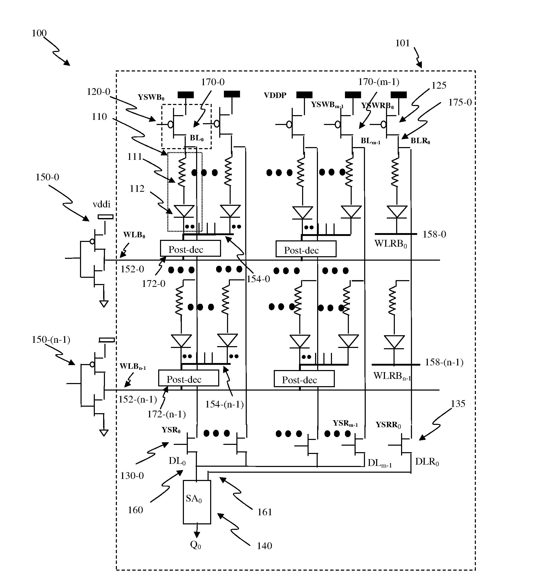
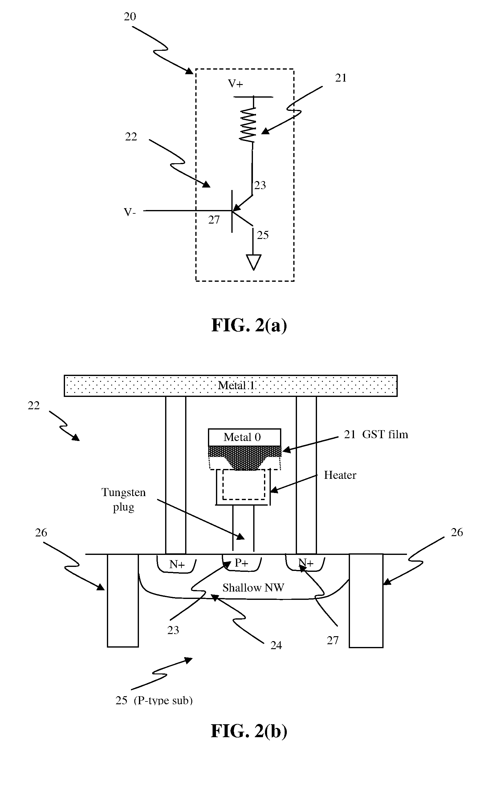
[0068]Embodiments disclosed herein use a polysilicon diode as program selector for a programmable resistive device. The diode can comprise P+ and N+ implants on a polysilicon substrate. Since the P+ and N+ implants and polysilicon are readily available in standard CMOS logic processes, these devices can be formed in an efficient and cost effective manner. There are no additional masks or process steps to save costs. The programmable resistive device can also be included within an electronic system.

[0069]FIG. 6(a) shows a block diagram of a memory cell 30 using a polysilicon diode according to one embodiment. In particular, the memory cell 30 includes a resistive element 31 and a polysilicon diode 32. The resistive element 31 can be coupled between an anode of the polysilicon diode 32 and a positive voltage V+. A cathode of the polysilicon diode 32 can be coupled to a negative voltage V−. In one implementation, the memory cell 30 can be a fuse cell with the resistive element 31 opera...


PUM


Abstract

Polysilicon diodes fabricated in standard CMOS logic processes can be used as program selectors for One-Time Programmable (OTP) devices, using electrical fuse, contact/via fuse, contact/via anti-fuse, or gate-oxide breakdown anti-fuse etc. as OTP element The diode can be constructed by P+/N+ implants on a polysilicon as a program selector. The OTP device has an OTP element coupled to a polysilicon diode. The OTP devices can be used to construct a two-dimensional OTP memory with the N-terminals of the diodes in a row connected as a wordline and the OTP elements in a column connected as a bitline. By applying a high voltage between a selected bitline and a selected wordline to turn on a diode in a selected cell for suitable duration of time, a current flows through an OTP element may change the resistance state. The cell data in the OTP memory can also be read by turning on a selected wordline and to couple a selected bitline to a sense amplifier. The wordlines may have high-resistivity local wordlines coupled to low-resistivity global wordlines through conductive contact(s) or via(s).

Description

CROSS-REFERENCE TO RELATED APPLICATIONS[0001]This application claims priority benefit of U.S. Provisional Patent Application No. 61 / 375,653, filed on Aug. 20, 2010 and entitled “Circuit and System of Using Junction Diode As Program Selector for Resistive Devices in CMOS Logic Processes,” which is hereby incorporated herein by reference; and U.S. Provisional Patent Application No. 61 / 375,660, filed on Aug. 20, 2010 and entitled “Circuit and System of Using Polysilicon Diode As Program Selector for Resistive Devices in CMOS Logic Processes,” which is hereby incorporated herein by reference.BACKGROUND OF THE INVENTION[0002]1. Field of the Invention[0003]The present invention relates to programmable memory devices, such as programmable resistive devices for use in memory arrays.[0004]2. Description of the Related Art[0005]A programmable resistive device is generally referred to a device's resistance states that may change after means of programming. Resistance states can also be determi...

Claims


Application Information

Patent Timeline
IPC IPC(8): G11C17/16G11C17/06
CPCG11C11/1659H01L27/2409G11C13/0004G11C13/0007G11C13/0011G11C13/0028G11C13/003G11C13/004G11C13/0069H01L29/785G11C11/1675G11C2013/0073G11C2213/72G11C2213/74G11C17/165G11C17/16H01L27/2436H01L45/06H01L45/144H01L45/04H01L45/085H01L45/1233H01L45/146H01L27/224G11C13/0002G11C8/14H10B61/10H10B63/20H10N70/231H10N70/826H10N70/8828H10B63/30H10N70/20H10N70/245H10N70/8833
Inventor CHUNG, SHINE C.
Owner ATTOPSEMI TECH CO LTD
Why Eureka
Try Eureka