Method for fabricating ceramic substrate

Active Publication Date: 2012-03-01
SEMCNS CO LTD
View PDF4 Cites 3 Cited by
  • Summary
  • Abstract
  • Description
  • Claims
  • Application Information

AI Technical Summary

Benefits of technology

[0009]An aspect of the present invention provides a method for forming a single or multiple polyimide surface layers of a ceramic substrate through a simpler process, and a method for fabricating a ceramic substrate using the same.

Problems solved by technology

However, when a commonly used printed circuit board (PCB) is employed for a small electronic component, drawbacks are recognized in that the PCB needs to be reduced in size, a signal loss occurs in a radio frequency area, and reliability is degraded in conditions of high temperature and high moisture.
However, due to the trend of an increase in the size of a semiconductor wafer and a ceramic substrate, the spin-coating method is not suitable for forming a uniform film of a weighty, large-scale substrate through a high speed rotation.

Method used


Image

  • Method for fabricating ceramic substrate
  • Method for fabricating ceramic substrate
  • Method for fabricating ceramic substrate

Examples


Embodiment Construction

[0031]Exemplary embodiments of the present invention will now be described in detail with reference to the accompanying drawings. The invention may however be embodied in many different forms and should not be construed as being limited to the embodiments set forth herein. Rather, these embodiments are provided so that this disclosure will be thorough and complete, and will fully convey the scope of the invention to those skilled in the art. In the drawings, the shapes and dimensions may be exaggerated for clarity, and the same reference numerals will be used throughout to designate the same or like components.

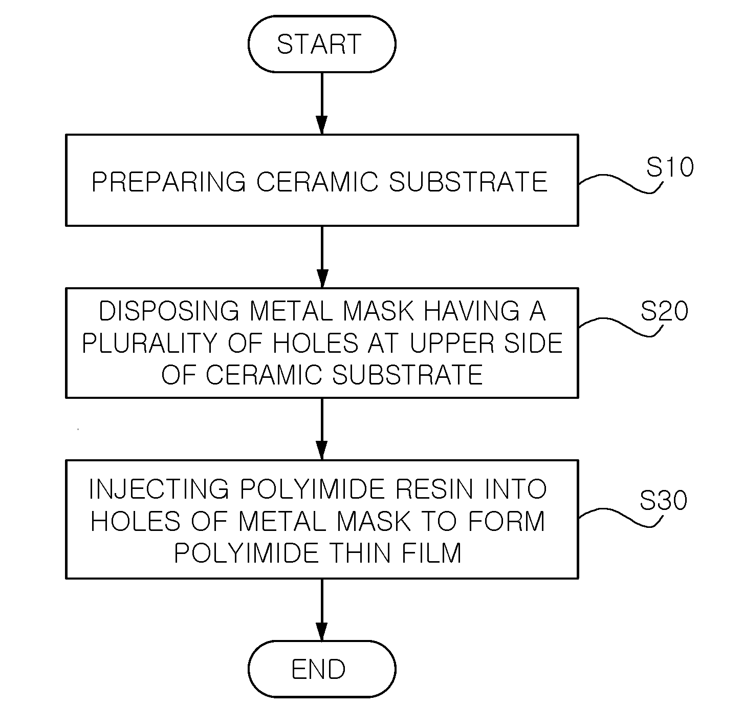
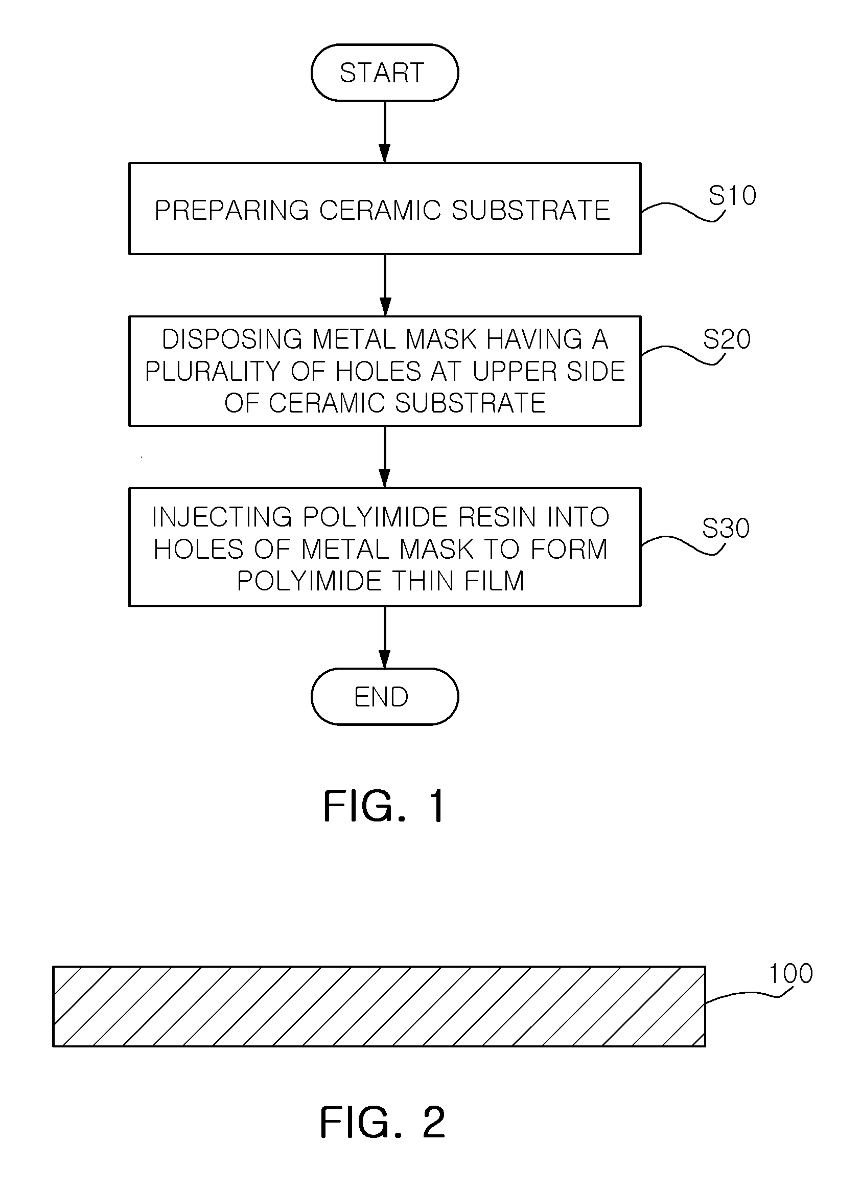
[0032]FIG. 1 is a flow chart illustrating the process of a method for forming a thin film on a ceramic substrate according to an exemplary embodiment of the present invention.

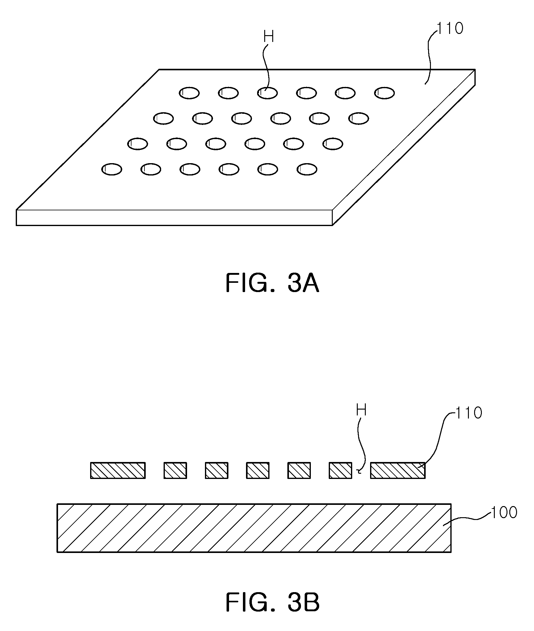
[0033]The method for forming a thin film on a ceramic substrate according to an exemplary embodiment of the present invention includes a step (S10) of preparing a ceramic substrate, a step (S20) of dispos...


PUM

PropertyMeasurementUnit
Fractionaaaaaaaaaa
Thicknessaaaaaaaaaa
Thicknessaaaaaaaaaa

Abstract

A method for fabricating a ceramic substrate includes: preparing a ceramic substrate; disposing a metal mask having a plurality of holes at an upper side of the ceramic substrate; and injecting a polyimide resin into the holes of the metal mask to form a polyimide thin film on the ceramic substrate. A thin film is formed on a ceramic substrate in a simpler manner, so the fabrication cost can be reduced and a fixed time can be shortened, thus increasing the efficiency of a product.

Description

CROSS-REFERENCE TO RELATED APPLICATIONS[0001]This application claims the priority of Korean Patent Application No. 10-2010-0082971 filed on Aug. 26, 2010, in the Korean Intellectual Property Office, the disclosure of which is incorporated herein by reference.BACKGROUND OF THE INVENTION[0002]1. Field of the Invention[0003]The present invention relates to a method for fabricating a ceramic substrate and, more particularly, to a method for forming a polyimide thin film on a large-scale, weighty ceramic substrate through a simple method.[0004]2. Description of the Related Art[0005]Recently, as electronic components continue to be reduced in size and smaller electronic components tend to be increasingly preferred, compact modules and substrates have been developed by making electronic components more precise, patterns finer, and films thinner. However, when a commonly used printed circuit board (PCB) is employed for a small electronic component, drawbacks are recognized in that the PCB n...

Claims


Application Information

Patent Timeline
IPC IPC(8): H05K3/10
CPCH05K3/0073H05K3/28H05K3/4629H05K2201/0154Y10T29/49126Y10T29/4913Y10T29/49155Y10T29/49144Y10T29/49165H05K2203/0759
Inventor SUNG, JE HONGCHOI, YOON HYUCK
Owner SEMCNS CO LTD
Why Eureka
Try Eureka