Semiconductor structure having conductive vias and method for manufacturing the same

a technology of conductive vias and semiconductors, applied in the direction of semiconductor devices, semiconductor/solid-state device details, electrical apparatus, etc., can solve the problems of increasing the length of the path that signals must traverse between chips, reducing the length of the package structure, and increasing the stack density

Active Publication Date: 2012-03-01
ADVANCED SEMICON ENG INC
View PDF2 Cites 46 Cited by
  • Summary
  • Abstract
  • Description
  • Claims
  • Application Information

AI Technical Summary

Problems solved by technology

This increases stack density, making the package structure smaller, and often reduces the length of the path that signals must traverse between chips.
However, thermal management of 3-D designs has been challenging.
Operating temperatures in excess of the limited operation temperature range results in chip performance drop, reduced reliability or damage.
In current chip processing the surface of the chip is covered with a protective layer, which has a low thermal conductivity and therefore hinders conducting of the heat from the chip interior, where it is produced, to the surrounding environment.
Even if the heat sink is disposed on the lower chip of the stacked-chip package structure, the protective layer likewise hinders thermal conductance between the lower chip and the heat sink, thus affecting operation and reliability of the stacked-chip package structure.

Method used


Image

  • Semiconductor structure having conductive vias and method for manufacturing the same
  • Semiconductor structure having conductive vias and method for manufacturing the same
  • Semiconductor structure having conductive vias and method for manufacturing the same

Examples


Embodiment Construction

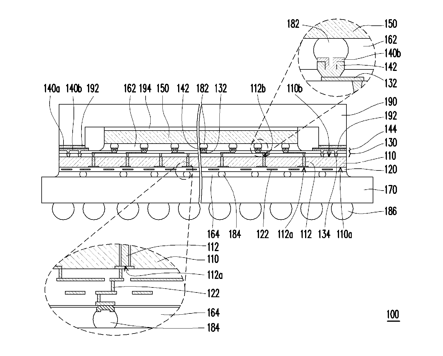
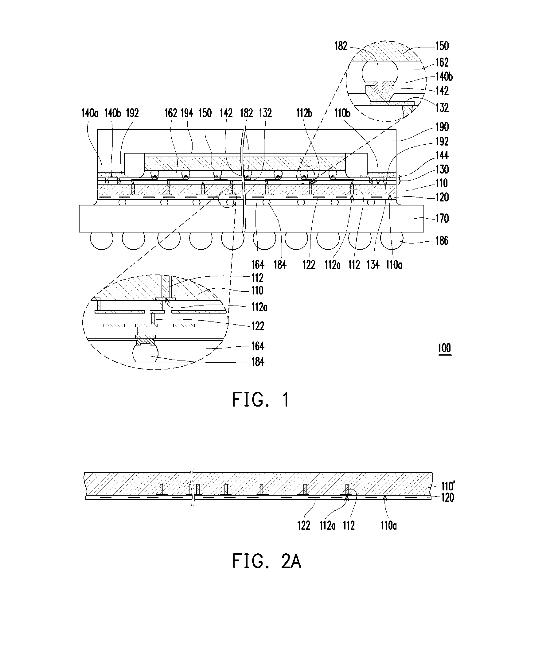
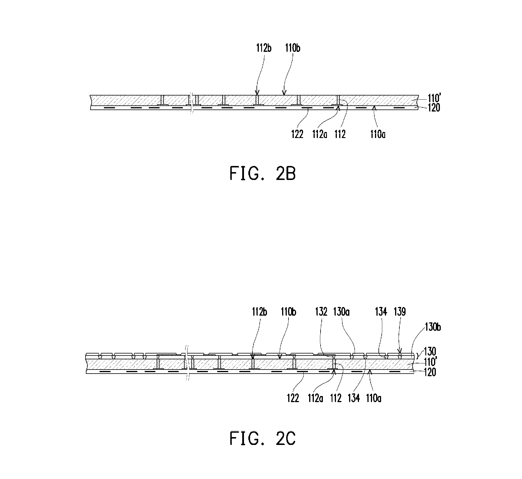
[0015]Referring to FIG. 1, there is shown a semiconductor structure 100 according to one embodiment of the present invention. The semiconductor structure 100 includes a first chip 110 having a plurality of through silicon vias (TSV) 112 in the semiconductor substrate thereof. It is to be appreciated that although silicon is the preferred semiconductor substrate material, the invention applies to any semiconductor material used in semiconductor chip fabrication, such as germanium, silicon germanium, gallium arsenide, or other III-V and II-IV compounds and the term is used generically throughout the disclosure regardless of the semiconductor material.

[0016]TSV fabrication can be placed into two main categories: “Via-First” processing and “Via-Last” processing. Via-First processing means that the through silicon vias are formed early in the manufacturing process, before the “back-end-of-line” (BEOL) processing. For Via-Last processing, the through silicon vias are fabricated after the ...


PUM


Abstract

A semiconductor structure includes a plurality of thermal vias and a heat dissipation layer disposed at a periphery of a back surface of a lower chip in a stacked-chip package. This arrangement improves solderability of a subsequently-bonded heat sink. Additionally, the thermal vias and the heat dissipation layer provide an improved thermal conduction path for enhancing heat dissipation efficiency of the semiconductor structure. A method for manufacturing the semiconductor structure is also provided.

Description

CROSS-REFERENCE TO RELATED APPLICATIONS[0001]This application claims the benefit of Taiwan application Serial No. 99129126, filed Aug. 30, 2010, the subject matter of which is incorporated herein by reference.BACKGROUND OF THE INVENTION[0002]1. Field of the Invention[0003]The present invention relates to the field of semiconductor packaging, and, more particularly, to thermal management of stacked-chip packages.[0004]2. Description of Related Art[0005]In stacked-chip packaging, multiple integrated circuit chips can be packaged in a single package structure in a vertically stacked manner. This increases stack density, making the package structure smaller, and often reduces the length of the path that signals must traverse between chips. Thus, stacked-chip packaging tends to increase the speed of signal transmission between or among chips. Additionally, stacked-chip packaging allows chips having different functions to be integrated in a single package structure. Use of through silicon...

Claims


Application Information

Patent Timeline
Patent Type & Authority Applications(United States)
IPC IPC(8): H01L23/498H01L21/50H01L23/48
CPCH01L21/563H01L2924/16235H01L23/49811H01L25/0657H01L2224/16225H01L2224/73204H01L2225/06513H01L2225/06517H01L2225/06541H01L2225/06572H01L2225/06589H01L2224/32225H01L2924/15311H01L23/3675H01L2224/97H01L2224/94H01L2224/73253H01L2224/32145H01L2224/16145H01L24/97H01L24/94H01L2924/00H01L2924/00012H01L2224/83H01L2224/81H01L2924/15787H01L2924/14
Inventor WANG, MENG-JEN
Owner ADVANCED SEMICON ENG INC
Why Eureka
Try Eureka