Flat Panel Display Panel and Method of Manufacturing the Same

a technology of display panel and flat panel, which is applied in the manufacture of electrode systems, electric discharge tubes/lamps, and discharge tubes luminescent screens, etc., can solve the problems of reducing the lifetime of the display panel, reducing the emission efficiency, or deteriorating the color of the emission light, and achieves the effect of improving mechanical strength

Inactive Publication Date: 2012-03-01
SAMSUNG DISPLAY CO LTD
View PDF6 Cites 27 Cited by
  • Summary
  • Abstract
  • Description
  • Claims
  • Application Information

AI Technical Summary

Benefits of technology

[0007]The present invention provides a flat panel display panel with improved mechanical strength and with the capability of absorbing impact by disposing an additional sealing member between a first substrate and a second substrate, and a method of manufacturing the flat panel display panel.

Problems solved by technology

In a flat panel display panel, a reduction in lifetime may be caused by oxidation or desquamation of an electrode material, etc. if moisture or oxygen penetrates into the flat panel display panel from a peripheral environment, and a reduction in emission efficiency or a deterioration in color of emission light may also be caused due to deterioration of a liquid crystal material of an organic material.

Method used


Image

  • Flat Panel Display Panel and Method of Manufacturing the Same
  • Flat Panel Display Panel and Method of Manufacturing the Same
  • Flat Panel Display Panel and Method of Manufacturing the Same

Examples


Embodiment Construction

[0037]The following descriptions and the attached drawings are provided to provide an understanding of the operations of the present invention, but some operations that can be easily realized by one of ordinary skill in the art may not be described.

[0038]Also, the present specification and the drawings are not provided to limit the scope of the invention which should be defined by the following claims. Terms used herein should be construed as having meanings and concepts corresponding to the technical concepts of the present invention in order to most appropriately describe the invention.

[0039]Hereinafter, the present invention will be described in detail by explaining embodiments of the invention with reference to the attached drawings.

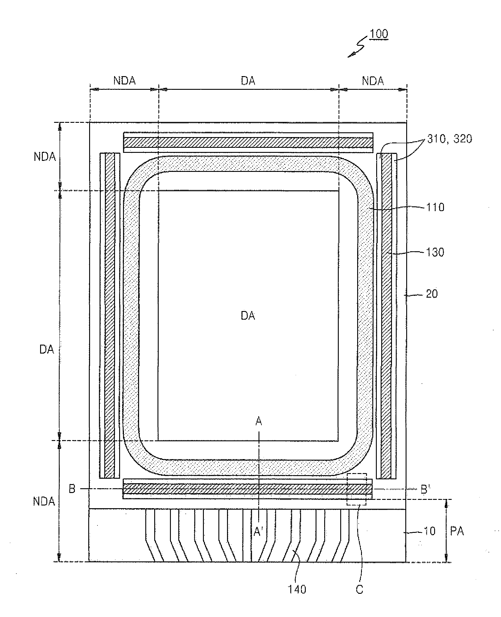
[0040]FIG. 1 is a plan view of a flat panel display panel 100 according to an embodiment of the present invention.

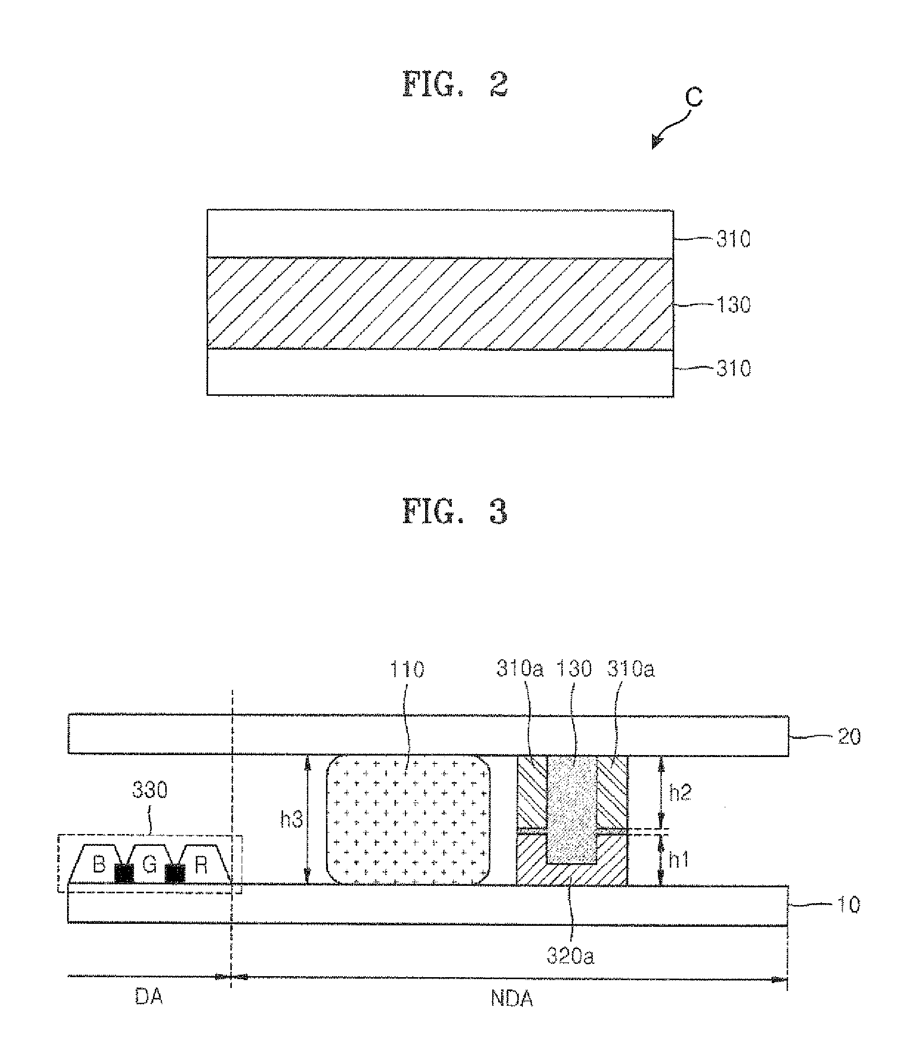
[0041]Referring to FIG. 1, the flat panel display panel 100 comprises a first substrate 10 including thin-film transistors (TFTs) and em...


PUM


Abstract

In a flat panel display panel and a method of manufacturing the same, the flat panel display panel may be constructed with a first substrate on which a plurality of pixels are formed; a second substrate disposed so as to face a surface of the first substrate on which the plurality of pixels are formed; a first sealing member disposed between the first and second substrates for sealing them; a first bank formed on the first substrate; a second bank formed on the second substrate and disposed facing the first bank; and a second sealing member disposed between the first and second banks.

Description

CLAIM OF PRIORITY[0001]This application makes reference to, incorporates the same herein, and claims all benefits accruing under 35 U.S.C. §119 from an application earlier filed in the Korean Intellectual Property Office on Sep. 1, 2010 and there duly assigned Serial No. 10-2010-0085503.BACKGROUND OF THE INVENTION[0002]1. Field of the Invention[0003]The present invention relates to a flat panel display panel and a method of manufacturing the same.[0004]2. Description of the Related Art[0005]Currently, display apparatuses tend to be replaced by portable and thin flat panel display devices. Flat panel display devices include liquid crystal display (LCD) devices, organic electroluminescence display devices, and plasma display panels (PDPs). A flat panel display panel included in a flat panel display device includes an LCD layer, an organic light-emitting diode (OLED), etc. disposed between a first substrate and a second substrate according to the type of flat panel display device, and ...

Claims


Application Information

Patent Timeline
Patent Type & Authority Applications(United States)
IPC IPC(8): H01J5/20H01J9/26
CPCH01L51/5246H01J9/241H10K50/8426H05B33/04
Inventor LEE, KYUNG-JUN
Owner SAMSUNG DISPLAY CO LTD
Why Eureka
Try Eureka