Clock frequency adjusting circuit and clock frequency adjusting method thereof

a clock frequency and clock frequency technology, applied in the direction of synchronous/start-stop systems, digital transmission, generating/distributing signals, etc., can solve the problems of increasing the manufacturing cost, requiring a longer adjustment time, and the above method is limited to a low-speed usb interface connection system. achieve the effect of reducing the manufacturing cos

Inactive Publication Date: 2012-03-01
PIXART IMAGING INC
View PDF2 Cites 13 Cited by
  • Summary
  • Abstract
  • Description
  • Claims
  • Application Information

AI Technical Summary

Benefits of technology

[0009]It is an object of the present invention to provide a method for automatically adjusting clock frequency and a clock frequency adjusting circuit, wherein an oscillator with an adjustable clock frequency is disposed inside the control IC of a USB device and the clock frequency of the oscillator is adjusted according to Keep Alive signals or SOF signals of the USB interface so as to effectively increase the accuracy of the clock frequency.
[0010]It is another object of the present invention to provide a method for automatically adjusting clock frequency and a clock frequency adjusting circuit, wherein it only needs to dispose an oscillator with an adjustable clock frequency inside the control IC of a USB device, without using a quartz oscillator, so as to decrease the cost, simplify the system circuit and reduce the size of the circuit board.
[0011]It is another object of the present invention to provide a clock frequency adjusting circuit and clock frequency adjusting method thereof, wherein an oscillator with an adjustable clock frequency is disposed inside the control IC of a USB device, and the clock frequency of the oscillator is adjusted according to a phase difference between SOF signals or EOP signals in a data stream from a USB host and a local signal of the USB device so as to effectively increase the accuracy of the clock frequency.
[0012]It is another object of the present invention to provide a clock frequency adjusting circuit and clock frequency adjusting method thereof that can be adapted to low-speed, full-speed and high-speed USB interfaces.
[0016]The clock frequency adjusting circuit and the clock frequency adjusting method of the present invention adjust the clock frequency according to EOP signals or SOF signals outputted by a USB host. Because the EOP signals and the SOF signals are regulated within a very small error range, they can be served as a reference for adjusting the clock frequency of the built-in oscillator of a USB device. In this manner, an additional quartz oscillator needs not to be installed in the USB device related to the present invention so as to effectively reduce the manufacturing cost.

Problems solved by technology

However, in the chip using a quartz oscillator, it is necessary to add additional 1˜2 pins to connect the quartz oscillator and therefore the cost will be increased.
However, the above circuit needs to use the whole signal package to adjust the output frequency and therefore it will take a longer adjustment time.
However, the above method is only limited to a low-speed USB interface connecting system.

Method used


Image

  • Clock frequency adjusting circuit and clock frequency adjusting method thereof
  • Clock frequency adjusting circuit and clock frequency adjusting method thereof
  • Clock frequency adjusting circuit and clock frequency adjusting method thereof

Examples


first embodiment

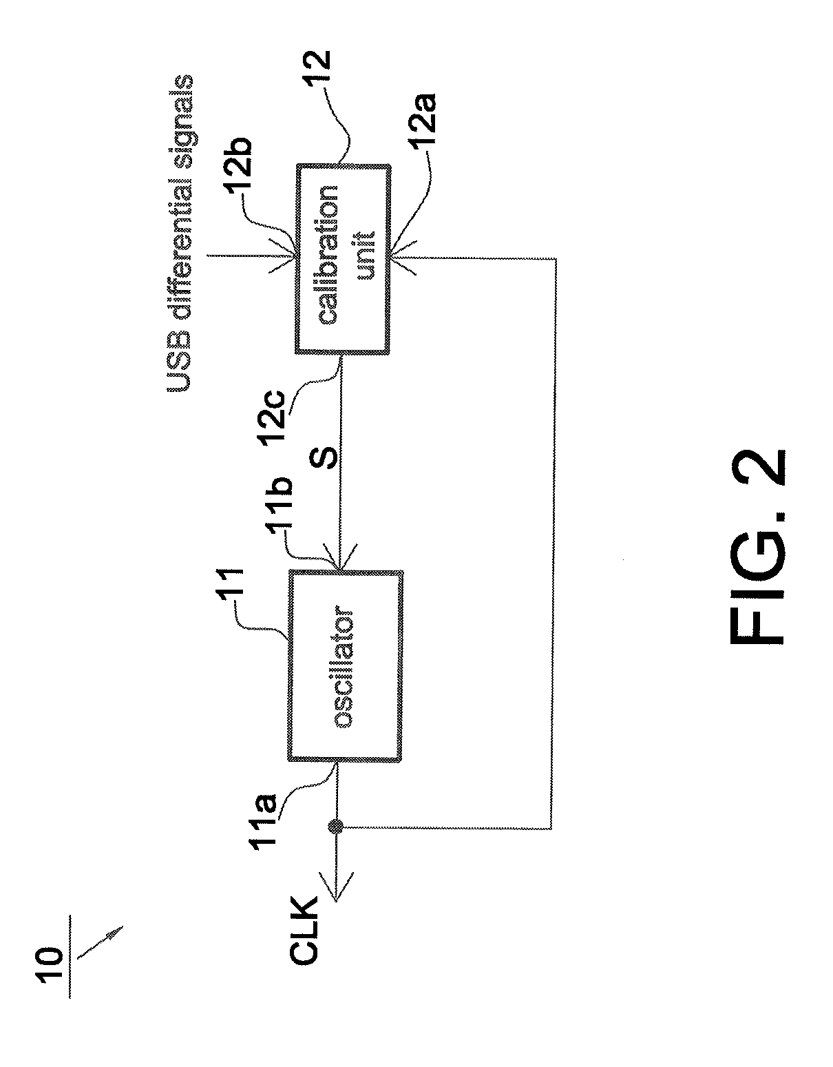
[0027]Referring to FIG. 2, it shows a block diagram of the clock frequency adjusting circuit 10 according to the present invention, wherein the clock frequency adjusting circuit 10 may be adapted to a USB device. The clock frequency adjusting circuit 10 includes an oscillator 11 and a calibration unit 12. The oscillator 11 is for generating a clock signal CLK with an adjustable clock frequency, and has an output 11a and an input 11b. The oscillator 11 may be, but not limited to, an RC oscillator.

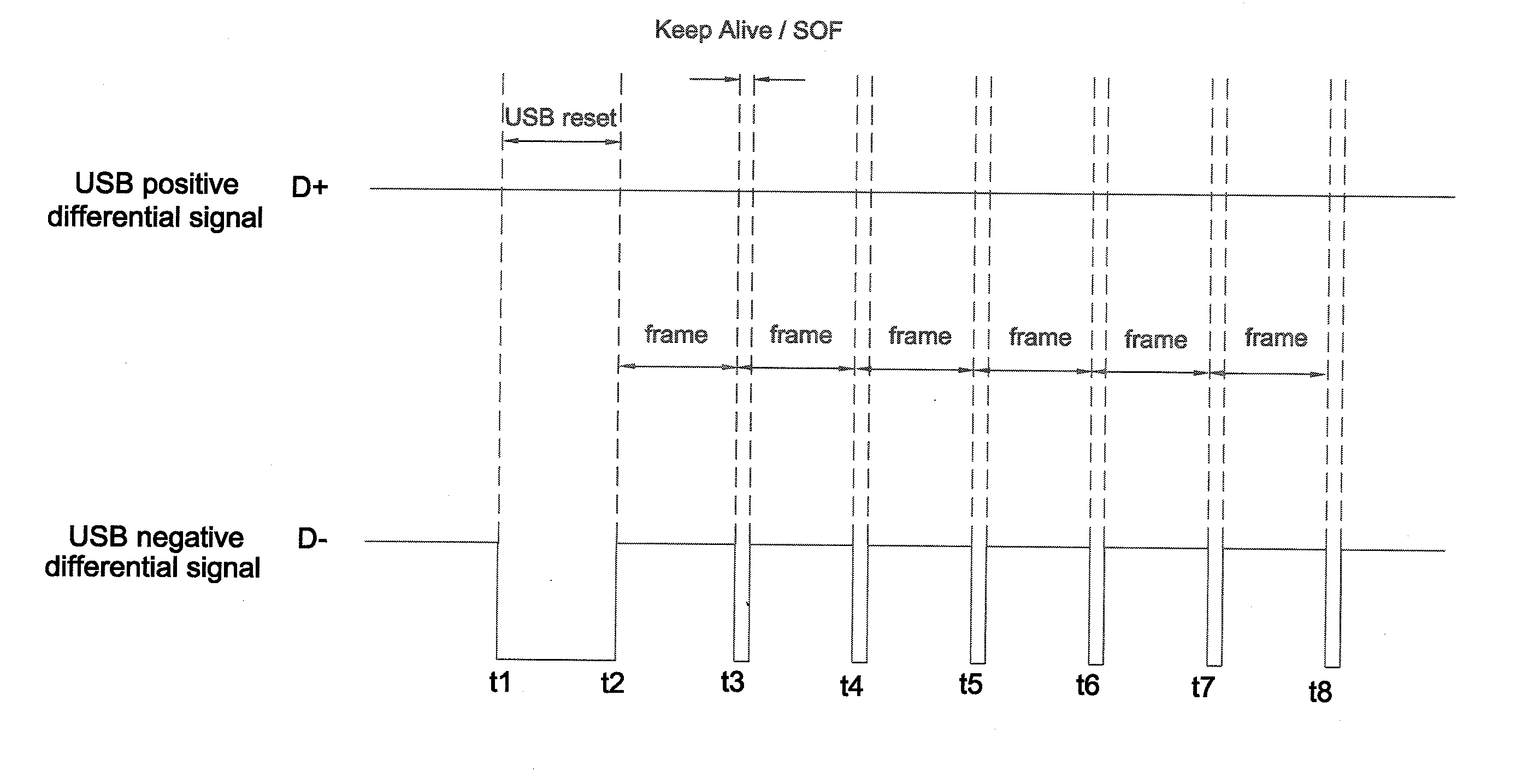
[0028]Referring to FIGS. 1 and 2 again, the calibration unit 12 is for outputting a control signal S to adjust the frequency of the clock signal CLK outputted from the oscillator 11, and includes a first input 12a, a second input 12b and a signal output 12c. The first input 12a receives the feedback signal of the clock signal CLK generated by the oscillator 11; the second input 12b receives USB differential signals from the USB system. The calibration unit 12 counts the clock signal CLK base...

second embodiment

[0032]Please refer to FIG. 4, it shows a block diagram of the clock frequency adjusting circuit 10′ according to the present invention. The clock frequency adjusting circuit 10′ includes a data receiver 13, a calibration unit 12′ and a clock generating circuit 11′. The data receiver 13 receives an external signal, such as a data stream from a USB host, and outputs a host signal SH, which includes SOF signals or EOP signals of the data stream. That is, the data receiver 13 retrieves SOF signals or EOP signals from the data stream.

[0033]The calibration unit 12′ includes a phase detector 121′ and a control circuit 122′, and has a first input 12a′, a second input 12b′ and a signal output 12c′. The phase detector 121′ is configured to receive the host signal SH from the data receiver 13 through the second input 12b′, and receive a local signal SL from the clock generating circuit 11′ through the first input 12a′, and calculate and output a phase difference ΔPhi between the host signal SH...


PUM


Abstract

A clock frequency adjusting method includes the steps of: calculating a phase difference between a local signal and SOF signals or EOP signals in an external signal; counting a count value of the phase difference based on a clock frequency of a local oscillator; and adjusting the clock frequency according to the count value. The present invention further provides a clock frequency adjusting circuit.

Description

CROSS REFERENCE TO RELATED APPLICATION[0001]This application is a continuation-in-part application of U.S. Ser. No. 12 / 261,436, filed on Oct. 30, 2008, the full disclosure of which is incorporated herein by reference.BACKGROUND OF THE INVENTION[0002]1. Field of the Invention[0003]This invention generally relates to a clock frequency adjusting circuit and clock frequency adjusting method thereof, and more particularly, to a clock frequency adjusting circuit and clock frequency adjusting method thereof that can automatically adjust the local oscillator of a USB device.[0004]2. Description of the Related Art[0005]A universal serial bus (USB) system is consisted of a USB host and a USB device connected by a USB interface, wherein the data transmission between the USB host and the USB device has to meet a data transmission specification. For example, in a high-speed device, data transmission needs to be controlled within a range of 480 MHz±0.05%; in a full-speed device, data transmission...

Claims


Application Information

Patent Timeline
Patent Type & Authority Applications(United States)
IPC IPC(8): H04L7/00
CPCG06F1/12
Inventor LIU, HSIANG SHENGCHANG, KUN CHIHCHEN, CHING CHIHSUN, CHIH PIN
Owner PIXART IMAGING INC
Why Eureka
Try Eureka