
Apparatus of manufacturing silicon carbide single crystal and method of manufacturing silicon carbide single crystal

Inactive Publication Date: 2012-03-15
BRIDGESTONE CORP
View PDF2 Cites 1 Cited by
  • Summary
  • Abstract
  • Description
  • Claims
  • Application Information

AI Technical Summary

Benefits of technology

[0005]Therefore, the present invention has been achieved in view of the above-described problems, and an object thereof is to provide an apparatus and a method of manufacturing a silicon carbide single crystal which prevent an occurrence of a crack from a contact portion between a single crystal and a guide member in a process of cutting the completely grown single crystal away from the guide member, even if the guide member is provided.
[0007]First, a feature of the present invention is summarized as an apparatus of manufacturing a silicon carbide single crystal, including: a crucible main body (crucible main body 11) which is opened at a top and accommodates a sublimation material (sublimation material 50) in a bottom portion (bottom portion 11a); a cover member (cover member 12) which covers an upper opening (upper opening 11b) of the crucible main body and is provided on a rear surface of the cover member with a seed crystal (seed crystal 60); and a cylindrical guide member (guide member 70) which is provided in the crucible main body to introduce a sublimated raw material gas from the sublimation material to the seed crystal and to guide growth of the silicon carbide single crystal when the silicon carbide single crystal is grown from the seed crystal, wherein the guide member includes a plurality of divided bodies (first divided body 74, second divided body 75). Consequently, since it has only to separate a plurality of divided bodies from each other when taking the completely grown single crystal off from the guide member, it is possible to easily take the single crystal off from the guide member and appropriately prevent the occurrence of the damage (e.g., a crack) of the single crystal.
[0010]According to the present invention, it is possible to provide an apparatus of manufacturing a silicon carbide single crystal capable of easily taking a single crystal off from a guide member and appropriately preventing the occurrence of the damage (e.g., a crack) of the single crystal, and to provide a method of manufacturing a silicon carbide single crystal.

Problems solved by technology

However, in the above-mentioned conventional art, since a grown single crystal is attached to the guide member, a crack may occur from a contact portion between the single crystal and the guide member when taking the completely grown single crystal off from the guide member and performing slicing machining for the single crystal.

Method used


Image

  • Apparatus of manufacturing silicon carbide single crystal and method of manufacturing silicon carbide single crystal
  • Apparatus of manufacturing silicon carbide single crystal and method of manufacturing silicon carbide single crystal
  • Apparatus of manufacturing silicon carbide single crystal and method of manufacturing silicon carbide single crystal

Examples


embodiment

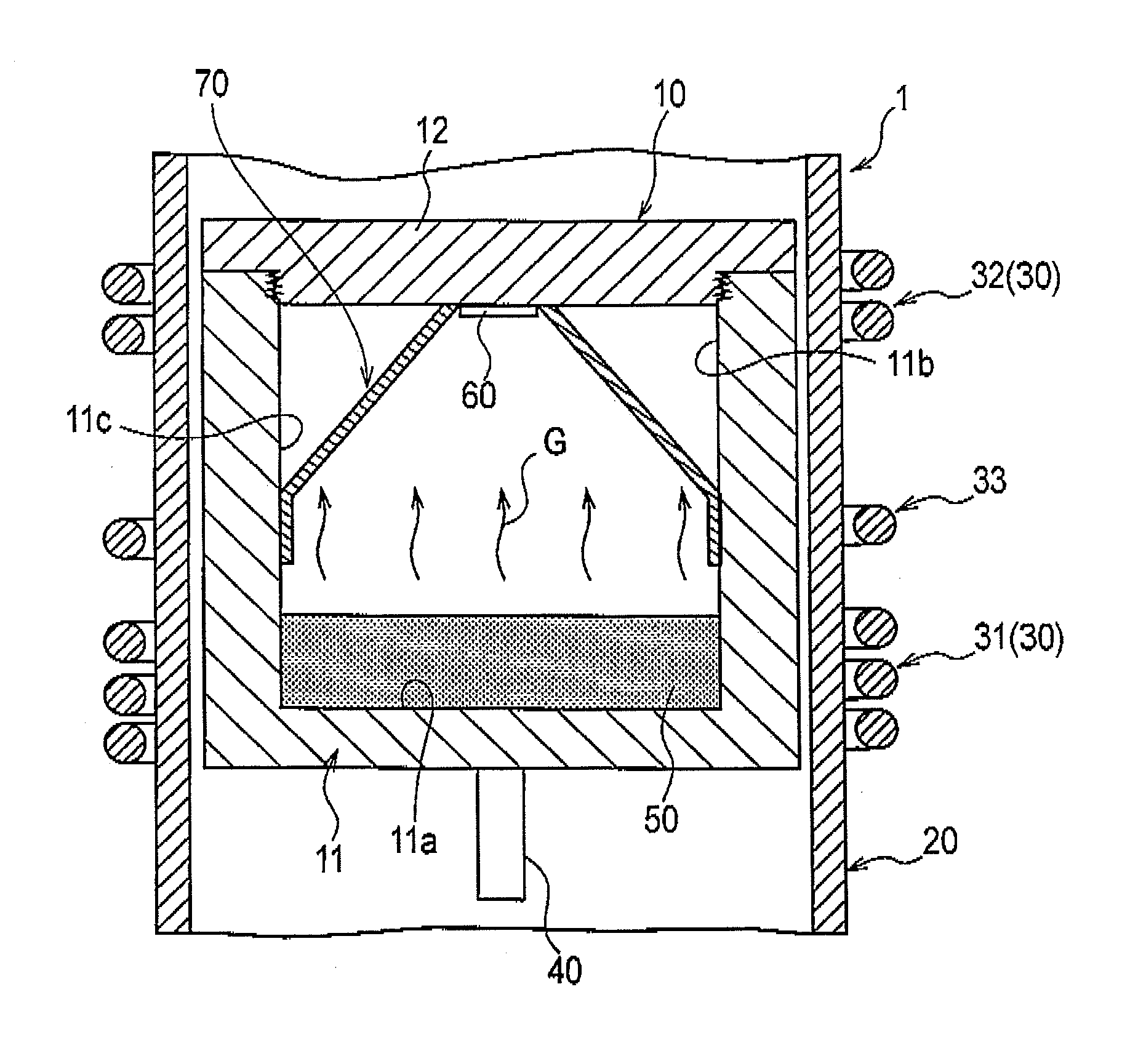
[0018]An apparatus of manufacturing a silicon carbide single crystal 1 according to an embodiment of the present invention will be described with reference to FIG. 1.

[0019]FIG. 1 is a sectional view illustrating the outline of the apparatus of manufacturing a silicon carbide single crystal according to the embodiment of the present invention.

[0020]As illustrated in FIG. 1, the apparatus of manufacturing a silicon carbide single crystal 1 includes a graphite crucible 10, a quartz tube 20 for covering at least the lateral side of the graphite crucible 10, and an induction heating coil 30 arranged at an outer periphery of the quartz tube 20.

[0021]The graphite crucible 10 includes a crucible main body 11, a cover member 12, and a guide member 70, and is fixed to the inside of the quartz tube 20 in a movable manner by a support rod 40.

[0022]A sublimation material 50 (powder including silicon carbide) is accommodated in the bottom portion 11a of the crucible main body 11. The cover member...

example

[0054]Next, in order to clarify the effect of the present invention, experimental results performed using apparatuses of manufacturing a silicon carbide single crystal according to a conventional example and an example will be described.

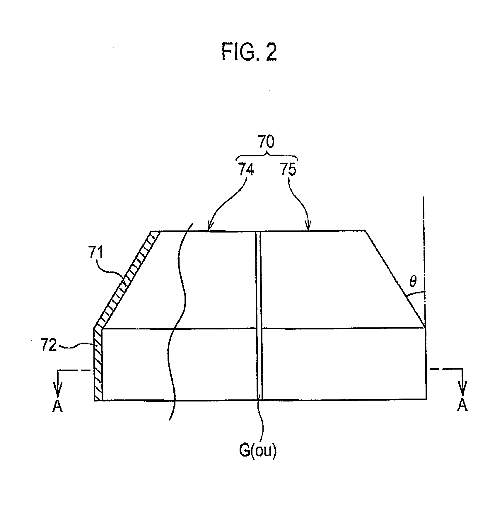
[0055]The manufacturing apparatuses according to the example used the guide member 70 illustrated in FIG. 1 and the manufacturing apparatuses according to the conventional example used a single-piece guide member instead of a divided type guide member.

[0056]In the example, first, the sublimation material 50 was contained in the bottom portion 11a of the crucible main body 11 and the seed crystal 60 was attached to the rear surface of the cover member 12. A current was allowed to flow through the first induction heating coil 31, the second induction heating coil 32, and the interference preventive coil 33 to heat the sublimation material 50 up to about 2112° C. for sublimation, thereby generating the raw material gas G. At this time, the pressure in t...


PUM


Abstract

Disclosed is an apparatus (1) for manufacturing a silicon carbide single crystal, which comprises: a crucible main body (11) that is opened at the top and holds a sublimation material (50) in the bottom portion (11a); a cover member (12) which covers the upper opening (11b) of the crucible main body (11); and a cylindrical guide member (70) which is provided in the crucible main body (11) for guiding the growth of the silicon carbide single crystal when the silicon carbide single crystal is grown from a seed crystal (60). The guide member (70) is separably configured of a first divided body and a second divided body.

Description

TECHNICAL FIELD[0001]The present invention relates to an apparatus of manufacturing a silicon carbide single crystal by using a sublimation recrystallization method and a method of manufacturing a silicon carbide single crystal.BACKGROUND ART[0002]Since a silicon carbide single crystal has better physical properties as compared with a generally used silicon single crystal and can be used for significantly improving the performance of an LED, a semiconductor device and the like, the silicon carbide single crystal is significantly expected as the next generation material. There has been disclosed an apparatus of manufacturing a silicon carbide single crystal (hereinafter, referred to as a single crystal, where appropriate) using a seed crystal and a sublimation material, which include silicon carbide. In general, the manufacturing apparatus includes a crucible main body for accommodating a powdery sublimation material including silicon carbide in the bottom portion thereof, a cover me...

Claims


Application Information

Patent Timeline
IPC IPC(8): C30B23/02C30B23/06
CPCC30B23/005C30B29/36
Inventor OKUNO, KENICHIRO
Owner BRIDGESTONE CORP
Features
  • Generate Ideas
  • Intellectual Property
  • Life Sciences
  • Materials
  • Tech Scout
  • Unparalleled Data Quality
  • Higher Quality Content
  • 60% Fewer Hallucinations
Learn More