High capacitance trench capacitor

a trench capacitor, high capacitance technology, applied in the direction of capacitors, semiconductor devices, electrical equipment, etc., can solve the problems of limited capacitance per unit area of a deep trench capacitor employing a conventional structure, difficult scaling of deep trench capacitors, and difficulty in maintaining the depth of a deep trench

Active Publication Date: 2012-03-15
GLOBALFOUNDRIES US INC
View PDF5 Cites 49 Cited by
  • Summary
  • Abstract
  • Description
  • Claims
  • Application Information

AI Technical Summary

Problems solved by technology

While deep trench capacitors provide a high capacitance per unit area, scaling of deep trench capacitors is difficult because maintaining the depth of a deep trench becomes m...

Method used


Image

  • High capacitance trench capacitor
  • High capacitance trench capacitor
  • High capacitance trench capacitor

Examples


first embodiment

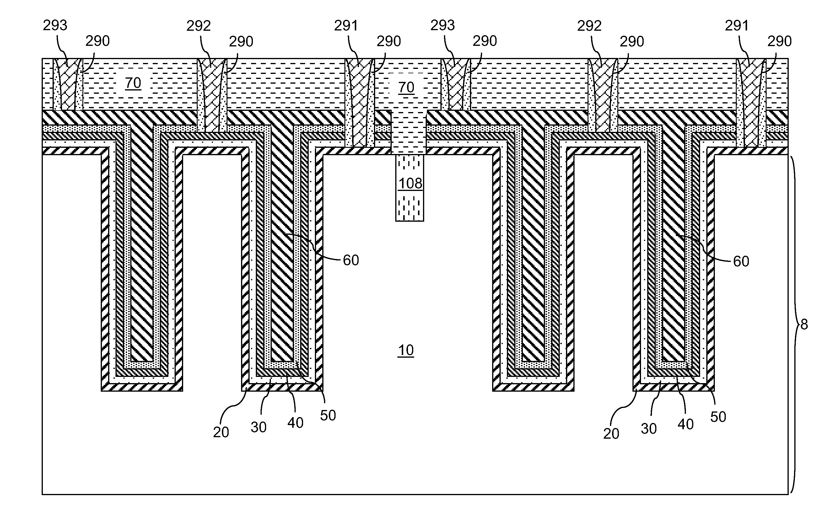
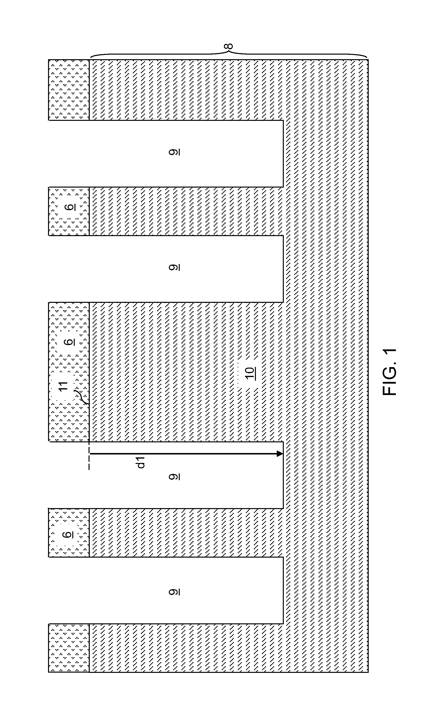
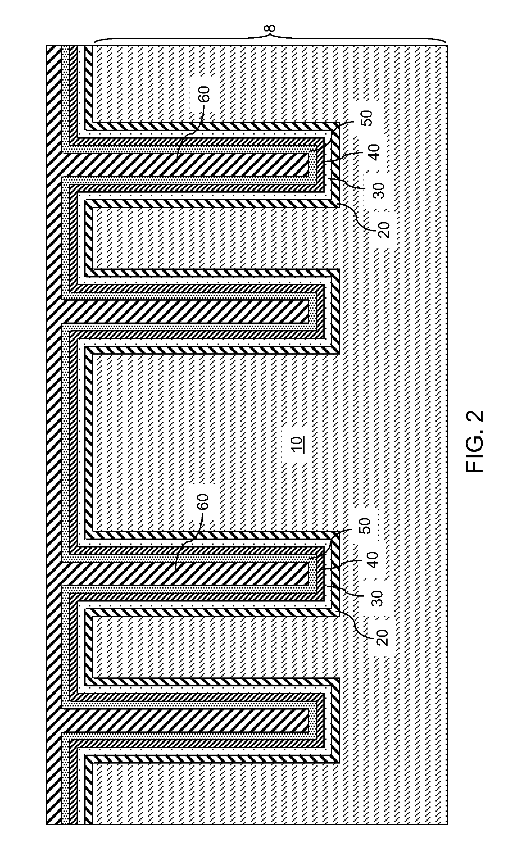
[0017]Referring to FIG. 1, a first exemplary structure according to the present disclosure includes a substrate 8, a mask layer 6, and at least one deep trench 9. The substrate 8 includes at least a substrate material layer 10 that includes a material having an electrical conductivity less than 103 siemens per centimeter (which is the same as 103 / Ohm·cm).

[0018]In one embodiment, the substrate material layer 10 is a semiconductor material layer having an electrical conductivity from 10−8 siemens per centimeter to 103 siemens per centimeter. For example, if the semiconductor material layer is a silicon layer, the semiconductor material layer can be an intrinsic silicon layer having an electrical conductivity less than 10−2 siemens per centimeter. Alternately, the semiconductor material layer can be a p-doped silicon layer or an n-doped silicon layer having a dopant concentration from about 1014 / cm3 to about 1020 / cm3 (corresponding to an electrical conductivity range from about 10−2 si...

second embodiment

[0050]Referring to FIG. 12, a second exemplary structure according to the present disclosure includes a substrate 8, a mask layer 6, and at least one deep trench 9. The substrate 8 includes at least a semiconductor material layer 110 that includes a semiconductor material having an electrical conductivity from 10−8 siemens per centimeter to 103 siemens per centimeter, and preferably having an electrical conductivity from 10−8 siemens per centimeter to 10 siemens per centimeter. For example, if the semiconductor material layer 110 is a silicon layer, the semiconductor material layer 110 can be an intrinsic silicon layer having an electrical conductivity less than 10−2 siemens per centimeter. Alternately, the semiconductor material layer 110 can be a p-doped silicon layer or an n-doped silicon layer having a dopant concentration from about 1014 / cm3 to about 1020 / cm3 (corresponding to an electrical conductivity range from about 10−2 siemens per centimeter to 103 siemens per centimeter)...


PUM


Abstract

A dual node dielectric trench capacitor includes a stack of layers formed in a trench. The stack of layers include, from bottom to top, a first conductive layer, a first node dielectric layer, a second conductive layer, a second node dielectric layer, and a third conductive layer. The dual node dielectric trench capacitor includes two back-to-back capacitors, which include a first capacitor and a second capacitor. The first capacitor includes the first conductive layer, the first node dielectric layer, the second conductive layer, and the second capacitor includes the second conductive layer, the second node dielectric layer, and the third conductive layer. The dual node dielectric trench capacitor can provide about twice the capacitance of a trench capacitor employing a single node dielectric layer having a comparable composition and thickness as the first and second node dielectric layers.

Description

BACKGROUND[0001]The present disclosure relates to a semiconductor structure, and particularly to a trench capacitor structure including dual node dielectric layers and methods of manufacturing the same.[0002]Deep trench capacitors are used in a variety of semiconductor chips for high areal capacitance and low device leakage. Typically, a deep trench capacitor provides a capacitance in the range from 4 fF (femto-Farad) to 120 fF. A deep trench capacitor can be employed as a charge storage unit in a dynamic random access memory (DRAM), which can be provided as a stand-alone semiconductor chip, or can be embedded in a system-on-chip (SoC) semiconductor chip. A deep trench capacitor can also be employed in a variety of circuit applications such as a charge pump or a capacitive analog component in a radio-frequency (RF) circuit.[0003]Deep trench capacitors are formed in a semiconductor substrate, which can be a semiconductor-on-insulator (SOI) substrate or a bulk substrate. Other semicon...

Claims


Application Information

Patent Timeline
IPC IPC(8): H01L29/92H01L21/02
CPCH01L27/10861H01L28/40H01L29/945H01L27/10867H10B12/038H10B12/0385
Inventor WONG, KEICH KWONG HONDIVAKARUNI, RAMACHANDRABOOTH, JR., ROGER A.
Owner GLOBALFOUNDRIES US INC
Why Eureka
Try Eureka