Physical quantity sensor
- Summary
- Abstract
- Description
- Claims
- Application Information
AI Technical Summary
Benefits of technology
Problems solved by technology
Method used
Image
Examples
first exemplary embodiment
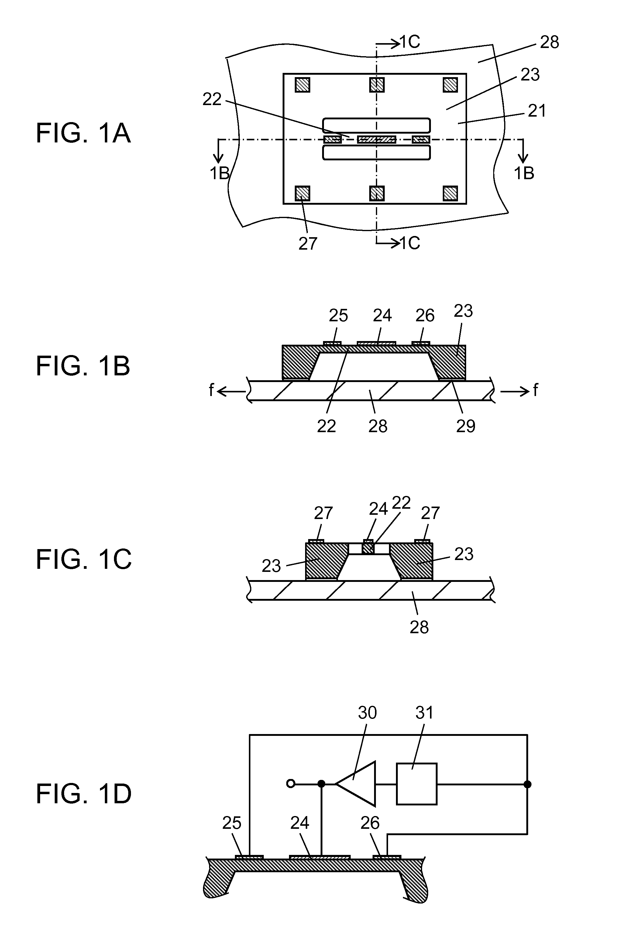
[0037]FIG. 1A is a top view of a physical quantity sensor in the first exemplary embodiment of the present invention. FIG. 1B is a sectional view taken along line 1B-1B in FIG. 1A. FIG. 1C is a sectional view taken along line 1C-1C in FIG. 1A. FIG. 1D illustrates an amplifier and a gain adjustment and phase shifting unit connected to the physical quantity sensor in FIG. 1B. In FIGS. 1A to 1D, semiconductor substrate 21 is typically made of silicon, and an insulating layer (not illustrated) of an oxide silicon layer or a silicon nitride layer is formed on its surface. Beam 22 is formed by etching semiconductor substrate 21. Beam 22 configures a beam-like vibrating body that changes its natural frequency by the action of physical quantity. Fixing part 23 surrounds beam 22, and supports both ends of the beam-like vibrating body. Driving element 24 (first piezoelectric element) is formed on a central portion of the surface of beam 22. Driving element 24 includes a lower electrode (not i...
second exemplary embodiment
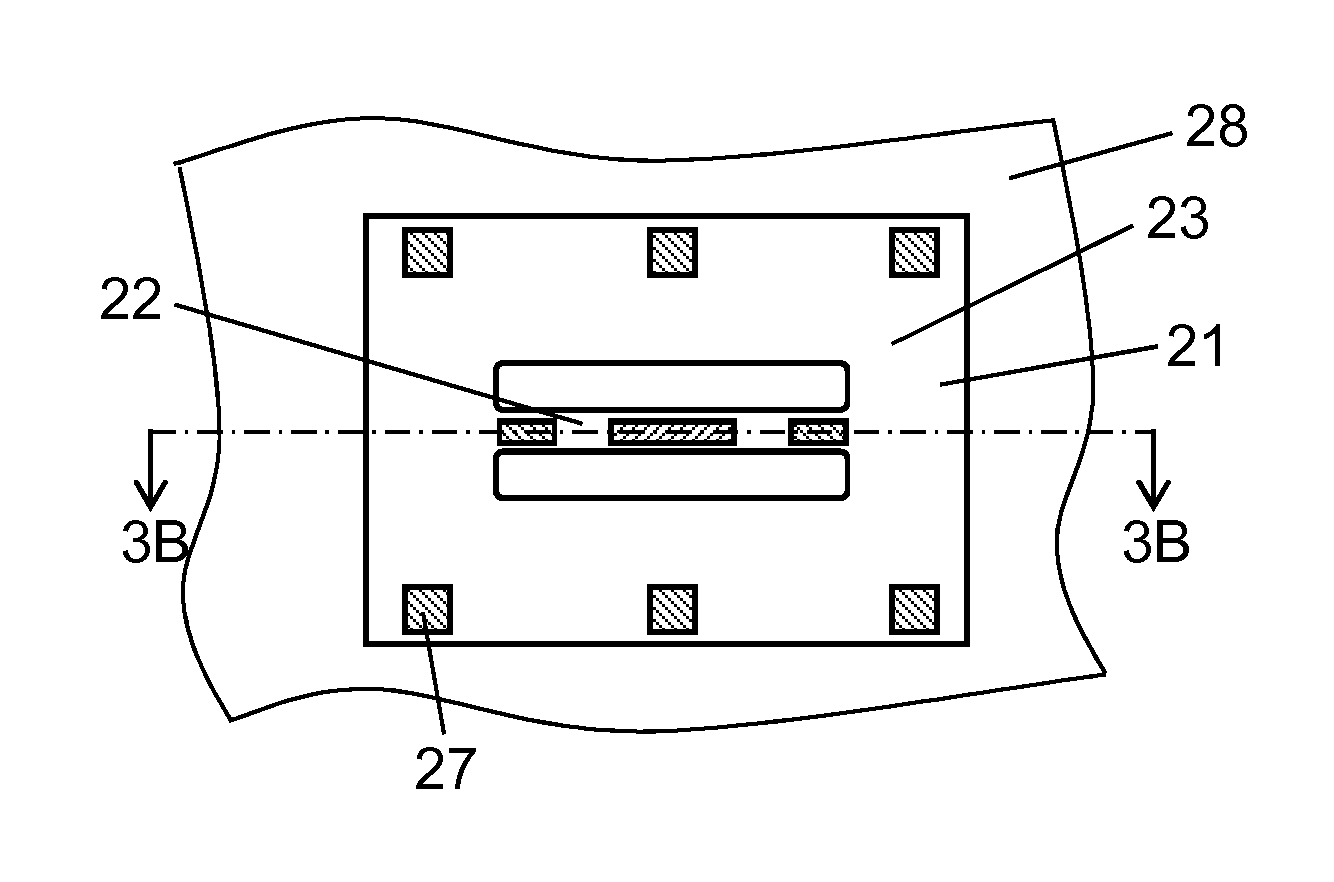
[0042]FIG. 3A is a top view of a physical quantity sensor in the second exemplary embodiment of the present invention. FIG. 3B is a sectional view taken along line 3B-3B in FIG. 3A. FIG. 3C illustrates an amplifier and a gain adjustment and phase shifting unit connected to the physical quantity sensor in FIG. 3B. In the second exemplary embodiment, same reference marks are given to components same as those in the first exemplary embodiment, and their description is omitted.
[0043]In FIGS. 3A to 3C, feedback element 40 (first piezoelectric element) is disposed on a central portion of beam 22. Feedback element 40 includes a lower electrode (not illustrated), a piezoelectric layer (not illustrated) typically made of PZT, and an upper electrode (not illustrated) in this sequence from the bottom. Driving elements 41 and 42 (second and third piezoelectric elements) are disposed on both ends of beam 22 at symmetrical positions relative to the center of beam 22. Each of driving elements 41 a...
third exemplary embodiment
[0048]FIG. 4A is a top view of a physical quantity sensor in the third exemplary embodiment of the present invention. FIG. 4B is a sectional view taken along line 4B-4B in FIG. 4A. FIG. 4C illustrates an amplifier and a gain adjustment and phase shifting unit connected to the physical quantity sensor in FIG. 4B. In the third exemplary embodiment, same reference marks are given to components same as those in the first exemplary embodiment, and their description is omitted.
[0049]In FIGS. 4A to 4C, detecting element 50 (first piezoelectric element) is disposed on a central portion of beam 22. Detecting element 50 includes a lower electrode (not illustrated), a piezoelectric layer (not illustrated) typically made of PZT, and an upper electrode (not illustrated) in this sequence from the bottom. Driving elements 51 and 52 (second and third piezoelectric elements) are disposed on both ends of beam 22 at symmetrical positions relative to the center of beam 22. Each of driving elements 51 a...
PUM
 Abstract
Description
Claims
Application Information


