Liquid Crystal Display Device with a Built-in Touch Screen and Method for Manufacturing the Same

a display device and touch screen technology, applied in the manufacture of electrode systems, electric discharge tubes/lamps, instruments, etc., can solve the problems of deteriorating yield, increased manufacturing costs, and easy operation of touch screen, so as to reduce the number of masks, reduce manufacturing costs, and improve driving efficiency

Active Publication Date: 2012-03-22
LG DISPLAY CO LTD
View PDF9 Cites 42 Cited by
  • Summary
  • Abstract
  • Description
  • Claims
  • Application Information

AI Technical Summary

Benefits of technology

[0033]An aspect of the present invention is to provide an LCD device with a built-in touch screen, which enhances driving efficiency by using a lower substrate of low-temperature poly silicon (LTPS), and a method for manufacturing the same.
[0034]Another aspect of the present invention is to provide an LCD device with a built-in touch screen, which reduces manufacturing costs by reducing the number of masks for a process of forming a lower substrate, and a method for manufacturing the same.
[0035]Another aspect of the present invention is to provide an LCD device with a built-in touch screen, which enhances manufacturing efficiency by simplifying a manufacturing process of a lower substrate, and a method for manufacturing the same.
[0036]Another aspect of the present invention is to provide an LCD device with a built-in touch screen, which enhances contact efficiency by increasing a contact between a data electrode and a pixel electrode on a lower substrate, and a method for manufacturing the same.

Problems solved by technology

Furthermore, easy operation of the touch screen rapidly enlarges the application field.
Accordingly, the process of forming the common electrode 75 is separately carried out from the process of forming the conductive line 76, whereby the manufacturing cost is increased and the yield is deteriorated due to the complicated manufacturing process.
Amorphous silicon (a-Si) TFT has disadvantages of low driving speed, and limitation in design of fine line width.
However, in comparison to the case of using the amorphous silicon (a-Si), the increased number of mask processes causes the complicated manufacturing process, to thereby deteriorate price competition and efficiency.

Method used


Image

  • Liquid Crystal Display Device with a Built-in Touch Screen and Method for Manufacturing the Same
  • Liquid Crystal Display Device with a Built-in Touch Screen and Method for Manufacturing the Same
  • Liquid Crystal Display Device with a Built-in Touch Screen and Method for Manufacturing the Same

Examples


first embodiment

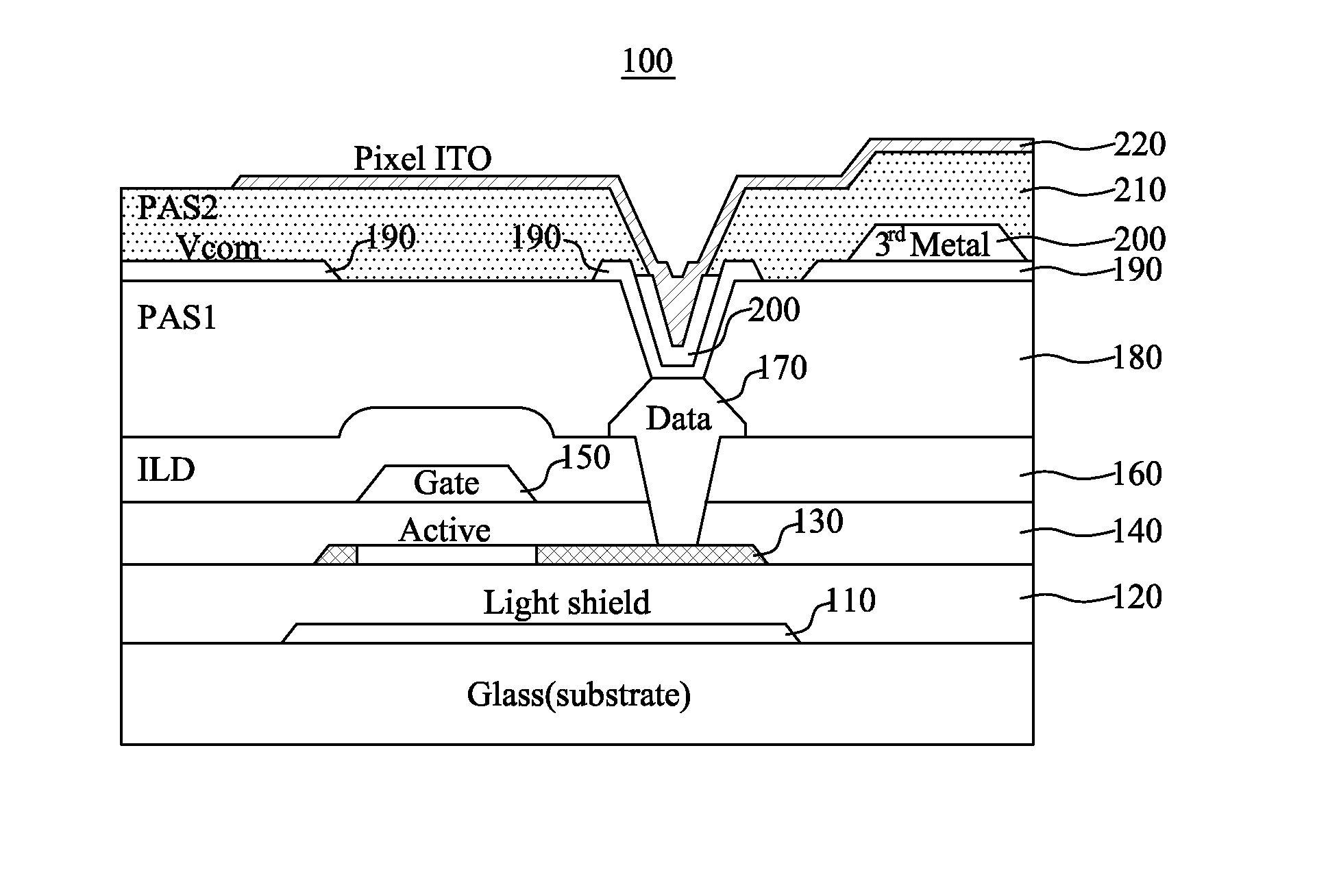
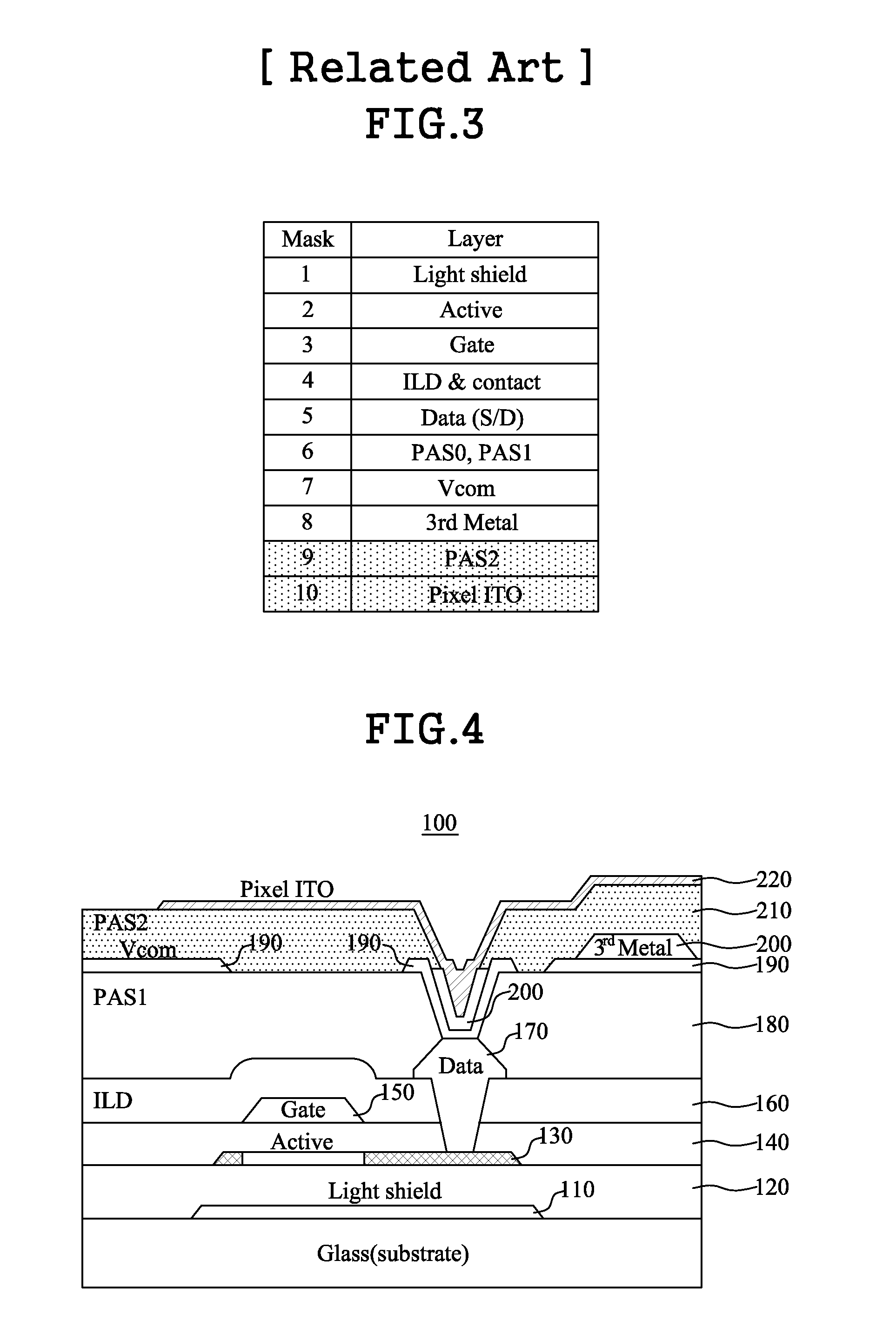
[0080]FIG. 4 illustrates a lower substrate in an LCD device with a built-in touch screen according to the present invention.

[0081]Referring to FIG. 4, plural pixels are formed on the lower substrate 100. Each pixel includes a thin film transistor (TFT); a pixel electrode 220; a common electrode 190; and a conductive line 200 for connection of the common electrodes 190 of the neighboring pixels.

[0082]At this time, the conductive line 200 functions as a contact line which makes the common electrode 190 driven as a touch-sensing electrode to detect a user's touch point.

[0083]In more detail, each pixel of the lower substrate 100 includes a light-shielding layer 110 on a glass substrate; a buffer layer 120 on the light-shielding layer 110; an active layer (semiconductor layer) 130 on the buffer layer 120; a gate insulating layer (GI) 140 on the active layer 130; and a gate electrode 150 partially overlapped with the active layer 130 and formed of metal on the gate insulating layer 140.

[0...

second embodiment

[0138]Hereinafter, an LCD device with a built-in touch screen according to the present invention will be described with reference to FIG. 10.

[0139]FIG. 10 illustrates a lower substrate in an LCD device with a built-in touch screen according to the second embodiment of the present invention. On explanation of a lower substrate 300 in the LCD device with a built-in touch screen according to the second embodiment of the present invention, a detailed explanation for the same parts as those of the first embodiment shown in FIG. 4 will be omitted.

[0140]Referring to FIG. 10, plural pixels are formed on a lower substrate 300.

[0141]The plural pixels include a thin film transistor (TFT), a pixel electrode 420, a common electrode 390, and a conductive line 400.

[0142]The conductive line 400 functions as a contact line which makes the common electrode 390 driven as a touch-sensing electrode to detect a user's touch point.

[0143]In more detail, each pixel of the lower substrate 300 includes an act...


PUM


Abstract

A liquid crystal display device with a built-in touch screen including a substrate having a pixel region, a thin film transistor formed in the pixel region, a first passivation layer formed on the thin film transistor, a first contact hole formed through a portion of the first passivation layer to expose the data electrode, a common electrode formed on at least one portion of the first passivation layer including inside the first contact hole, the common electrode operable to sense touch, a conductive line formed on at least one portion of the first passivation layer including inside the first contact hole, a second passivation layer formed on the common electrode and the conductive line, a second contact hole formed through a portion of the second passivation layer to expose the conductive line corresponding to the data electrode, and a pixel electrode electrically connected with the conductive line, the pixel electrode formed on the second passivation layer and inside the second contact hole, wherein the second passivation layer and the pixel electrode are simultaneously formed by a mask process using a half-tone mask.

Description

CROSS REFERENCE TO RELATED APPLICATIONS[0001]This application claims the benefit of the Korean Patent Application No. 10-2010-0092385 filed on Sep. 20, 2010, which is hereby incorporated by reference as if fully set forth herein.BACKGROUND OF THE INVENTION[0002]1. Field of the Invention[0003]The present invention relates to a flat panel display device, and more particularly, a liquid crystal display device with a built-in touch screen, which improves driving efficiency and reduces manufacturing costs by having a simplified manufacturing process, and a method for manufacturing the same.[0004]2. Discussion of the Related Art[0005]With the developments in various mobile electronic equipment such as mobile terminals and notebook computers, there is an increasing demand for an applicable flat panel display device.[0006]The flat panel display device may include a liquid crystal display device (LCD), a plasma display panel (PDP), a field emission display device (FED), a light-emitting diod...

Claims


Application Information

Patent Timeline
Patent Type & Authority Applications(United States)
IPC IPC(8): G06F3/041H01J9/00
CPCG02F1/13338G02F2001/13629G02F2001/136231G06F3/0412G02F2001/136295G02F2001/136236G02F1/136227G06F3/044G06F3/0443G02F1/136231G02F1/136236G02F1/13629G02F1/136295G02F1/13439G02F1/136286G02F1/1368G02F1/13625H01L27/1288
Inventor OH, KUM MILEE, HAN SEOKPARK, WON KEUN
Owner LG DISPLAY CO LTD
Why Eureka
Try Eureka