

Multilayer ceramic electronic component and a method for manufacturing the same
a multi-layer ceramic and electronic component technology, applied in the direction of fixed capacitor details, line/current collector details, electrical equipment, etc., can solve the problems of multi-layer ceramic capacitors that the adhesive strength between the ceramic green sheet forming the side gap region and the green chip is not sufficient, and the multi-layer ceramic capacitors cannot be multi-layer ceramic capacitors. , to achieve the effect of preventing peeling (gap peeling) between the green chip
- Summary
- Abstract
- Description
- Claims
- Application Information
AI Technical Summary
Benefits of technology
Problems solved by technology
Method used
Image

Examples
Embodiment Construction
[0041]Hereinafter, for description of preferred embodiments of the present invention, as a multilayer ceramic electronic component, a multilayer ceramic capacitor will be described by way of example.
[0042]FIGS. 1 to 9 are views illustrating a first preferred embodiment of the present invention.
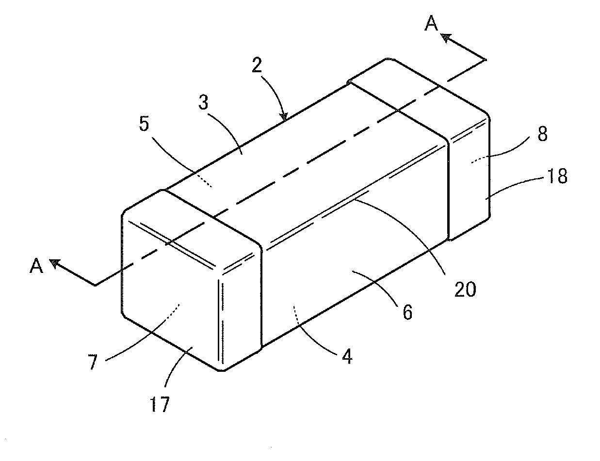
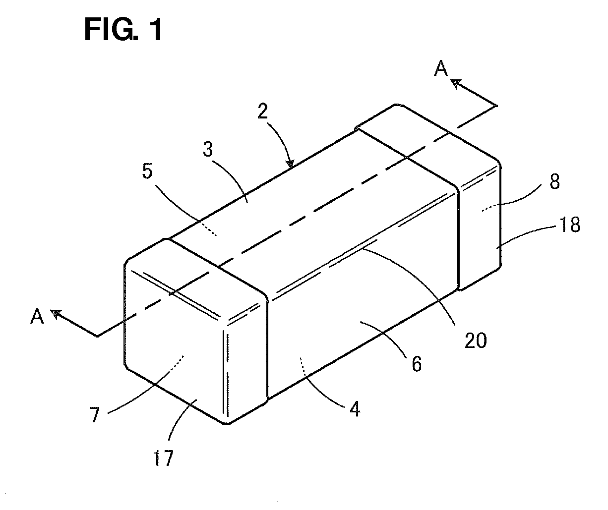
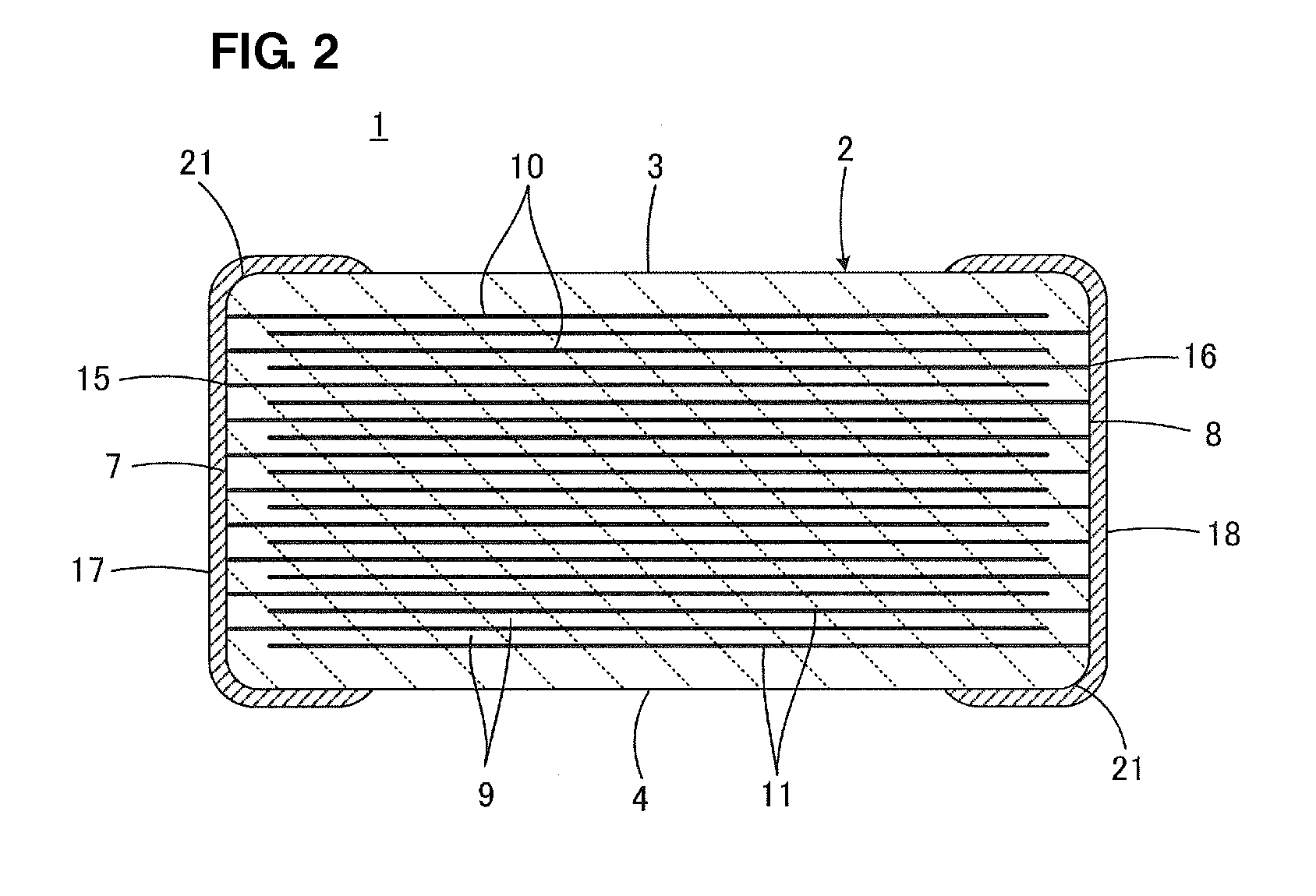
[0043]First, as shown in FIGS. 1 to 5, a multilayer ceramic capacitor 1 includes an element body 2. The element body 2 includes one pair of principal surfaces 3 and 4 facing each other, one pair of side surfaces 5 and 6 facing each other, and one pair of end surfaces 7 and 8 facing each other and has an approximately rectangular parallelepiped shape, for example.
[0044]As shown in FIGS. 2 and 5, the element body 2 includes a laminate portion 12 of a laminate structure including a plurality of ceramic layers 9 extending in the direction of the principal surfaces 3 and 4 and laminated in the direction perpendicular or substantially perpendicular to the principal surfaces 3 and 4 and a plurality o...
PUM
| Property | Measurement | Unit |
|---|---|---|
| thickness | aaaaa | aaaaa |
| thickness | aaaaa | aaaaa |
| curvature radius Rd | aaaaa | aaaaa |
Abstract
Description
Claims
Application Information