Semiconductor Device Die with Integrated MOSFET and Low Forward Voltage Diode-Connected Enhancement Mode JFET and Method

a technology of semiconductor devices and enhancement modes, applied in the direction of solid-state devices, transistors, transportation and packaging, etc., can solve the problems of high assembly cost and high manufacturing cost, short switching recovery time is not a very important performance parameter, and incurs a large overall package size and associated

Active Publication Date: 2012-03-29
ALPHA & OMEGA SEMICON INC
View PDF1 Cites 21 Cited by
  • Summary
  • Abstract
  • Description
  • Claims
  • Application Information

AI Technical Summary

Benefits of technology

[0008]A semiconductor device die with integrated metal oxide semiconductor field effect transistor (MOSFET) and diode-connected enhancement mode junction field effect transistor (JFET) is proposed. The semiconductor device die may include two conduction nodes (or terminals) Terminal-S, Terminal-D and a control node (or terminal) Terminal-Gate. The MOSFET-JFET semiconductor device die includes:

Problems solved by technology

While a Schottky diode boasts the advantage of very short switching recovery time, it is remarked that for the application of battery charging the short switching recovery time is not a very important performance parameter.
With two die pads (2a and 2b) and two dies (2c and 2d), the MOSFET-Schottky diode Co-package 2 undesirably incurs a large overall package size and associated high assembly cost and high manufacturing cost.

Method used


Image

  • Semiconductor Device Die with Integrated MOSFET and Low Forward Voltage Diode-Connected Enhancement Mode JFET and Method
  • Semiconductor Device Die with Integrated MOSFET and Low Forward Voltage Diode-Connected Enhancement Mode JFET and Method
  • Semiconductor Device Die with Integrated MOSFET and Low Forward Voltage Diode-Connected Enhancement Mode JFET and Method

Examples


Embodiment Construction

[0093]The description above and below plus the drawings contained herein merely focus on one or more currently preferred embodiments of the present invention and also describe some exemplary optional features and / or alternative embodiments. The description and drawings are presented for the purpose of illustration and, as such, are not limitations of the present invention. Thus, those of ordinary skill in the art would readily recognize variations, modifications, and alternatives. Such variations, modifications and alternatives should be understood to be also within the scope of the present invention.

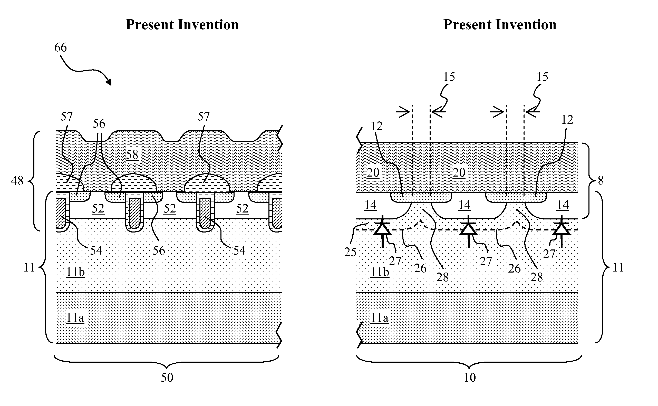
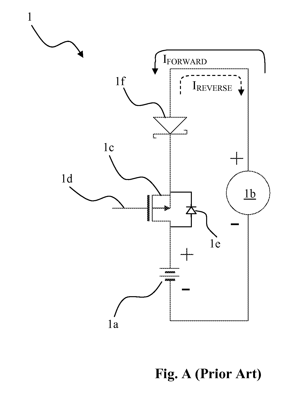
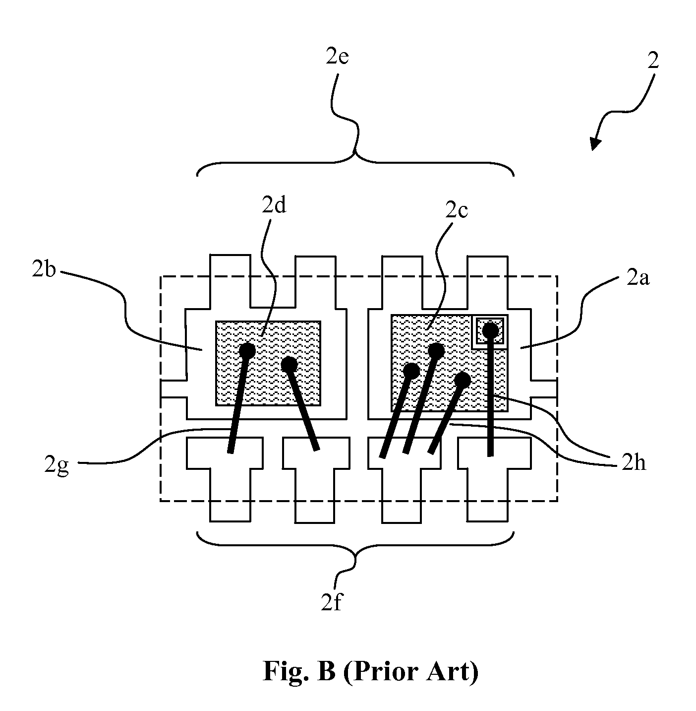
[0094]FIG. 1A through FIG. 1C illustrate the cross sectional semiconductor die structure of a diode-connected P-channel enhancement mode junction field effect transistor (DCE-JFET) 10 of the present invention, together with its simplified equivalent circuit 36 and P-channel DCE-JFET circuit representation 38. A DCE-JFET device region 8 is located at the top of a lower common semiconduct...


PUM


Abstract

A semiconductor die with integrated MOSFET and diode-connected enhancement mode JFET is disclosed. The MOSFET-JFET die includes common semiconductor substrate region (CSSR) of type-1 conductivity. A MOSFET device and a diode-connected enhancement mode JFET (DCE-JFET) device are located upon CSSR. The DCE-JFET device has the CSSR as its DCE-JFET drain. At least two DCE-JFET gate regions of type-2 conductivity located upon the DCE-JFET drain and laterally separated from each other with a DCE-JFET gate spacing. At least a DCE-JFET source of type-1 conductivity located upon the CSSR and between the DCE-JFET gates. A top DCE-JFET electrode, located atop and in contact with the DCE-JFET gate regions and DCE-JFET source regions. When properly configured, the DCE-JFET simultaneously exhibits a forward voltage Vf substantially lower than that of a PN junction diode while the reverse leakage current can be made comparable to that of a PN junction diode.

Description

FIELD OF INVENTION[0001]This invention relates generally to the field of semiconductor device structure. More specifically, the present invention is directed to device structure and manufacturing method to form an integrated power semiconductor device useful in a battery charging circuit.BACKGROUND OF THE INVENTION[0002]A prior art battery charging circuit 1, by way of example useful in cell phone battery charging application, is depicted in Fig. A. A battery charging source Vcharge 1b is provided with its negative terminal connected to the negative terminal of a battery 1a. The positive terminal of the battery charging source Vcharge 1b is bridged to the positive terminal of the battery 1a with a serial connection of a Schottky diode DS 1f and a power Metal-Oxide-Semiconductor Field Effect Transistor (MOSFET) 1c, in this case a P-channel MOSFET, with a built-in body diode 1e and a gate control signal Vcontrol 1d. While in some situations the built-in body diode 1e is advantageous, ...

Claims


Application Information

Patent Timeline
Patent Type & Authority Applications(United States)
IPC IPC(8): H02J7/00H01L21/8232H01L27/06
CPCH01L27/098H01L27/0617
Inventor LUI, SIKWANG, WEI
Owner ALPHA & OMEGA SEMICON INC
Why Eureka
Try Eureka