Detection apparatus and radiation detection system

a detection apparatus and radiation detection technology, applied in the field of detection apparatus and radiation detection system, can solve the problems of difficult to reduce the turn-on period, difficult to reduce the design necessary period of the switch element, dull or distorted driving pulse transmitted via the driving line, etc., to reduce the capacitance of the signal line, reduce noise, and increase the driving speed

Inactive Publication Date: 2012-04-05
CANON KK
View PDF5 Cites 6 Cited by
  • Summary
  • Abstract
  • Description
  • Claims
  • Application Information

AI Technical Summary

Benefits of technology

[0012]In view of the above, the present invention provides a technique to achieve a further reduction in noise by a reduction in signal line capacitance and an increase in driving speed by a reduction in time constant associated with a driving line in a detection apparatus, in particular in a stacked-type detection apparatus with a greater number of pixels arranged at smaller intervals.
[0014]By virtue of the above structure, in the detection apparatus and more particularly in the stacked-type detection apparatus according to one aspect of the present invention, a reduction in noise is achieved by reducing the capacitance associated with the signal line, and an increase in driving speed is achieved by reducing the time constant associated with the driving line.

Problems solved by technology

This can cause a driving pulse transmitted via the driving line to become dull or distorted.
Therefore, if the turn-on period of the switch element is reduced, the dullness can make it difficult for the switch element to be in an on-state for a designed necessary period.
That is, the dullness makes it difficult to reduce the turn-on period, which makes it difficult to increase the driving speed.
In particular, in a stacked-type detection apparatus such as that disclosed in U.S. Patent Application No. 2009 / 0004768, an increase also occurs in the number of intersects between signal lines and conversion elements, which causes a further increase in capacitance associated with signal lines.
As a result, noise caused by the capacitance associated with the signal lines increases, which results in a reduction in sensitivity.

Method used


Image

  • Detection apparatus and radiation detection system
  • Detection apparatus and radiation detection system
  • Detection apparatus and radiation detection system

Examples


first embodiment

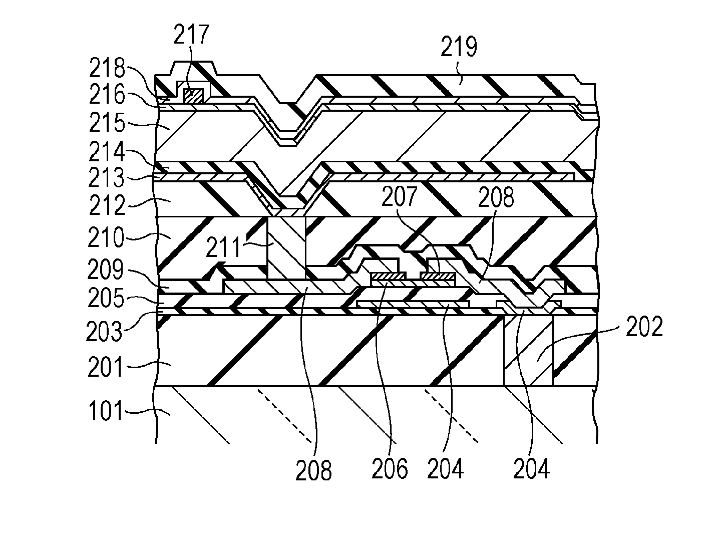
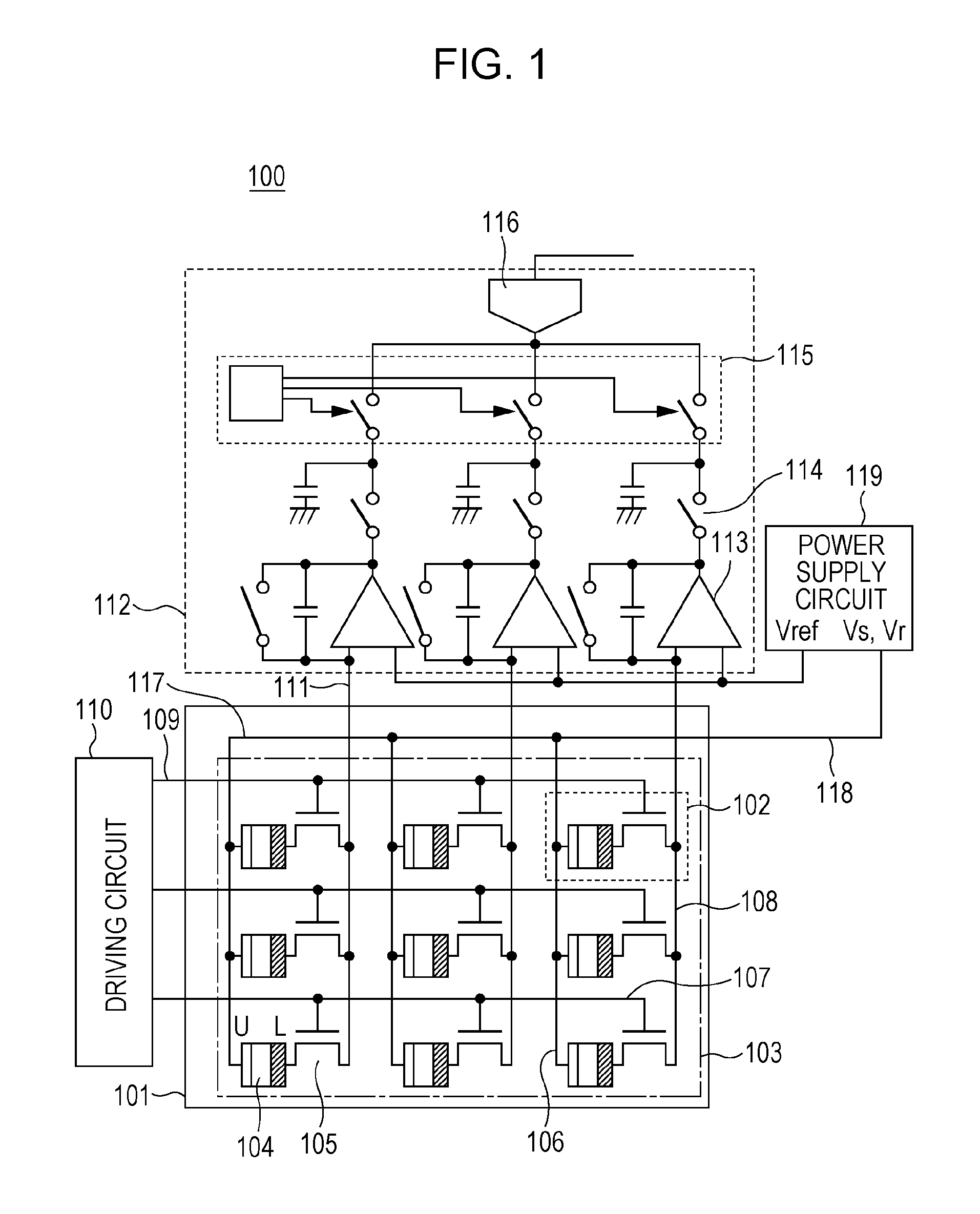
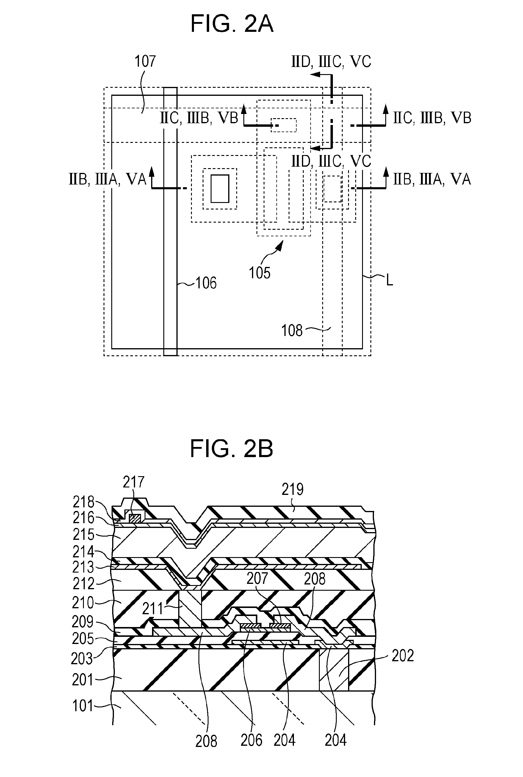
[0023]A radiation detection apparatus according to a first embodiment is described below with reference to FIG. 1 and FIGS. 2A to 2D. A radiation detection apparatus 100 according to the first embodiment includes an insulating substrate 101 such as a glass substrate and a pixel region 103 formed on the insulating substrate 101. In the pixel region 103, a plurality of pixels 102 are arranged in a matrix having row and column directions. Each pixel 102 includes a conversion element 104 configured to convert radiation or light into an electric charge, and a switch element 105 configured to output an electric signal corresponding to the electric charge. In the present embodiment, a metal-insulator-semiconductor type (MIS-type) photoelectric conversion element is used as the conversion element, and a thin film transistor (TFT) is used as the switch element. In a case where the conversion element is designed to convert light into an electric charge, a fluorescent member is disposed on (st...

second embodiment

[0033]A second embodiment of the present invention is described below with reference to FIGS. 4A to 4D. FIG. 4A is a plan view of a pixel of a radiation detection apparatus according to the second embodiment of the present invention, and FIGS. 4B to 4D are cross-sectional views taken along lines IVB-IVB, IVC-IVC, and IVD-IVD, respectively, in FIG. 4A. The equivalent circuit and the operation principle of the radiation detection apparatus are similar to those according to the first embodiment, and thus a further description thereof is omitted.

[0034]The present embodiment is different from the first embodiment in that shapes of the signal line 108 and the driving line 107 are controlled. Line capacitance of the signal line 108 occurs at an intersection between the signal line 108 and the driving line 107 and at an intersection between the signal line 108 and the first electrode L of the conversion element 104. In each case, capacitance occurs between the signal line 108 and a conducti...

third embodiment

[0036]A third embodiment of the present invention is described below with reference to FIGS. 5A to 5C. FIG. 5A is a cross-sectional view taken along line VA-VA of FIG. 2A, FIG. 5B is a cross-sectional view taken along line VB-VB of FIG. 2A, and FIG. 5C is a cross-sectional view taken along line VC-VC of FIG. 2A. The equivalent circuit and the operation principle of the radiation detection apparatus are similar to those according to the first embodiment, and thus a further description thereof is omitted.

[0037]The present embodiment is different from the first embodiment in that the signal line 108 and the control electrode of the switch element 105 are both formed by the first conductive layer 202 embedded in the first insulating layer 201. By forming both the signal line 108 and the control electrode of the switch element 105 using the first conductive layer 202, it becomes possible to simplify the production process compared with that according to the first embodiment, which allows...


PUM


Abstract

A stacked-type detection apparatus includes a plurality of pixels arranged in a matrix having row and column directions. Each pixel includes a conversion element configured to convert radiation or light into an electric charge, and a switch element configured to output an electric signal corresponding to the electric charge. A driving line is connected to switch elements arranged in the row direction, and a signal line is connected to switch elements arranged in the column direction. In each pixel, the conversion element is disposed above the switch element. The signal line is formed by a conductive layer embedded in an insulating layer located below an uppermost surface portion of a main electrode of the switch element located below an uppermost surface portion of the driving line located below the conversion element.

Description

BACKGROUND OF THE INVENTION[0001]1. Field of the Invention[0002]The present invention relates to a detection apparatus applicable to a medical imaging apparatus, a non-destructive testing apparatus, an analysis apparatus using radiation, or the like, and also relates to a radiation detection apparatus and a radiation detection system.[0003]2. Description of the Related Art[0004]In recent years, great advances have been made in technology to produce a liquid crystal display panel using thin film transistors (TFTs), which has allowed it to achieve a large-sized display panel or a large-sized display screen. This technology is also applicable to production of a large-sized area sensor (detection apparatus) having a conversion element such as a photoelectric conversion element realized using semiconductor and a switch element such as a TFT. Such an area sensor may be combined with a fluorescent member to perform a wavelength conversion, i.e., to convert a radiation such as a X-ray into ...

Claims


Application Information

Patent Timeline
Patent Type & Authority Applications(United States)
IPC IPC(8): G01T1/20
CPCG01T1/247G01T1/24H04N5/32H01L27/14663
Inventor FUJIYOSHI, KENTAROMOCHIZUKI, CHIORIWATANABE, MINORUISHII, TAKAMASAKAWANABE, JUNWAYAMA, HIROSHI
Owner CANON KK
Why Eureka
Try Eureka