Composite material, light-emitting element, light-emitting device, electronic device, and lighting device

a technology of light-emitting elements and composite materials, which is applied in the direction of luminescent compositions, organic semiconductor devices, thermoelectric devices, etc., can solve the problems of power consumption, difficult to obtain features, and low emission efficiency of light-emitting elements, and achieve high carrier-transport properties, high carrier-injection properties, and high emission efficiency

Active Publication Date: 2012-04-05
SEMICON ENERGY LAB CO LTD
View PDF4 Cites 44 Cited by
  • Summary
  • Abstract
  • Description
  • Claims
  • Application Information

AI Technical Summary

Benefits of technology

[0049]According to one embodiment of the present invention, it is possible to provide a composite material including an organic compound and an inorganic compound and having a high carrier-transport property. It is also possible to provide a composite material having a high carrier-injection property to an organic compound. It is also possible to provide a composite material in which light absorption due to charge transfer interaction is unlikely to occur.
[0050]According to one embodiment of the present invention, it is possi

Problems solved by technology

This feature is difficult to obtain with point light sources typified by incandescent lamps and LEDs or linear light sources typified by fluorescent lamps.
On the other hand, there are many issues regarding light-emitting elements using organic EL.
One of the issues is a reduction in power consumption.
However, as described in Non-Patent Document 1, PANI has a problem that transmittance becomes poor when a film thickness becomes thick.
In other words, since the problem is with the transparency of the material itself that is used for the buffer layer

Method used


Image

  • Composite material, light-emitting element, light-emitting device, electronic device, and lighting device
  • Composite material, light-emitting element, light-emitting device, electronic device, and lighting device
  • Composite material, light-emitting element, light-emitting device, electronic device, and lighting device

Examples


embodiment 1

[0100]In this embodiment, a composite material of one embodiment of the present invention will be described.

[0101]A composite material of one embodiment of the present invention is a composite material of an organic compound having a particular skeleton and an inorganic compound. There is no limitation for a preparation method of the composite material of one embodiment of the present invention; for example, it can be formed by a co-evaporation method where the organic compound and the inorganic compound are deposited at the same time. The mixing ratio, in mass ratio, of the organic compound to the inorganic compound in the composite material of one embodiment of the present invention is preferably approximately 8:1 to 1:2 (=Organic compound:inorganic compound), and more desirably, 4:1 to 1:1 (=Organic compound:inorganic compound). When the composite material is formed by a co-evaporation method, the mixing ratio can be controlled by separately adjusting the deposition rates for the...

embodiment 2

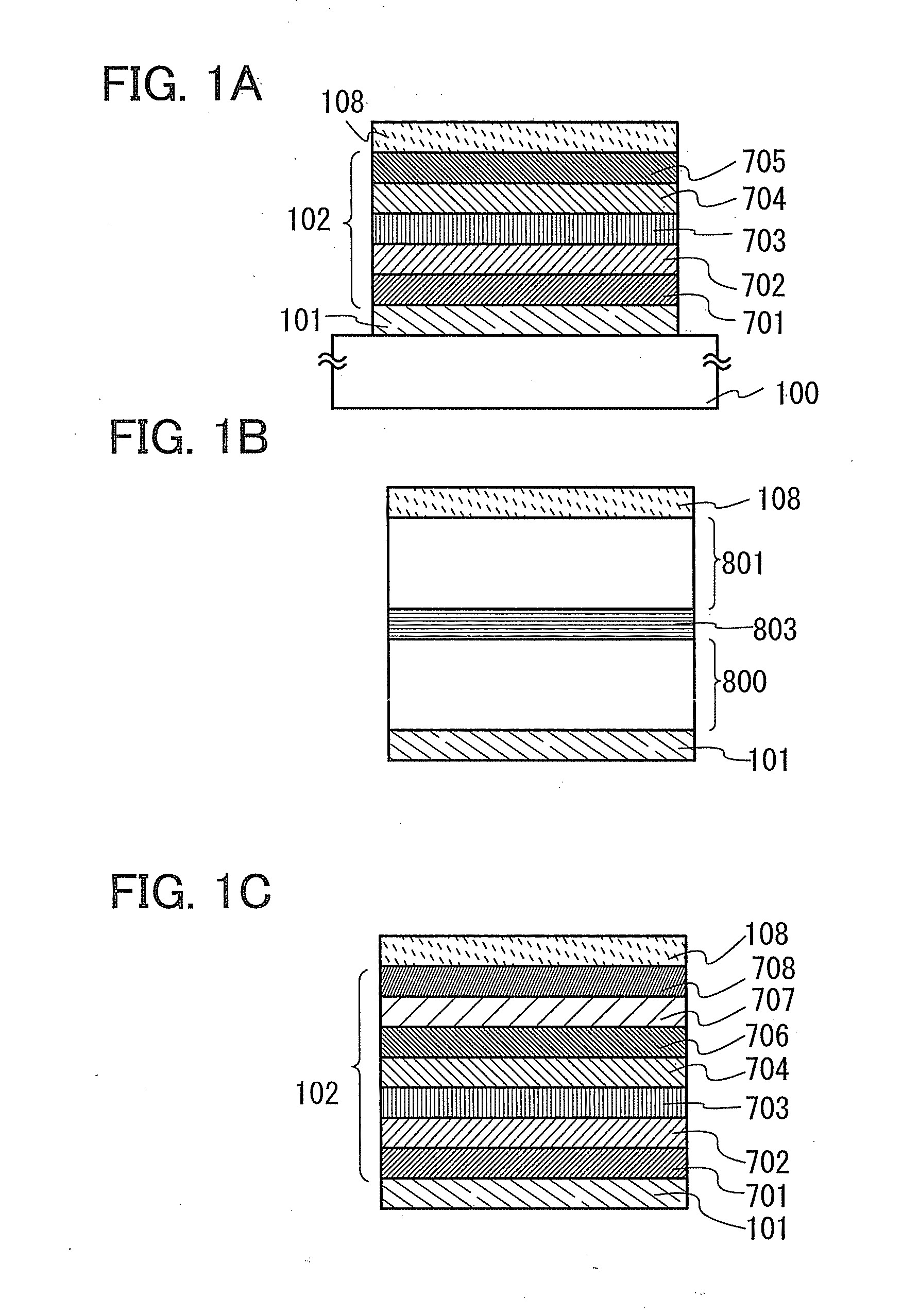
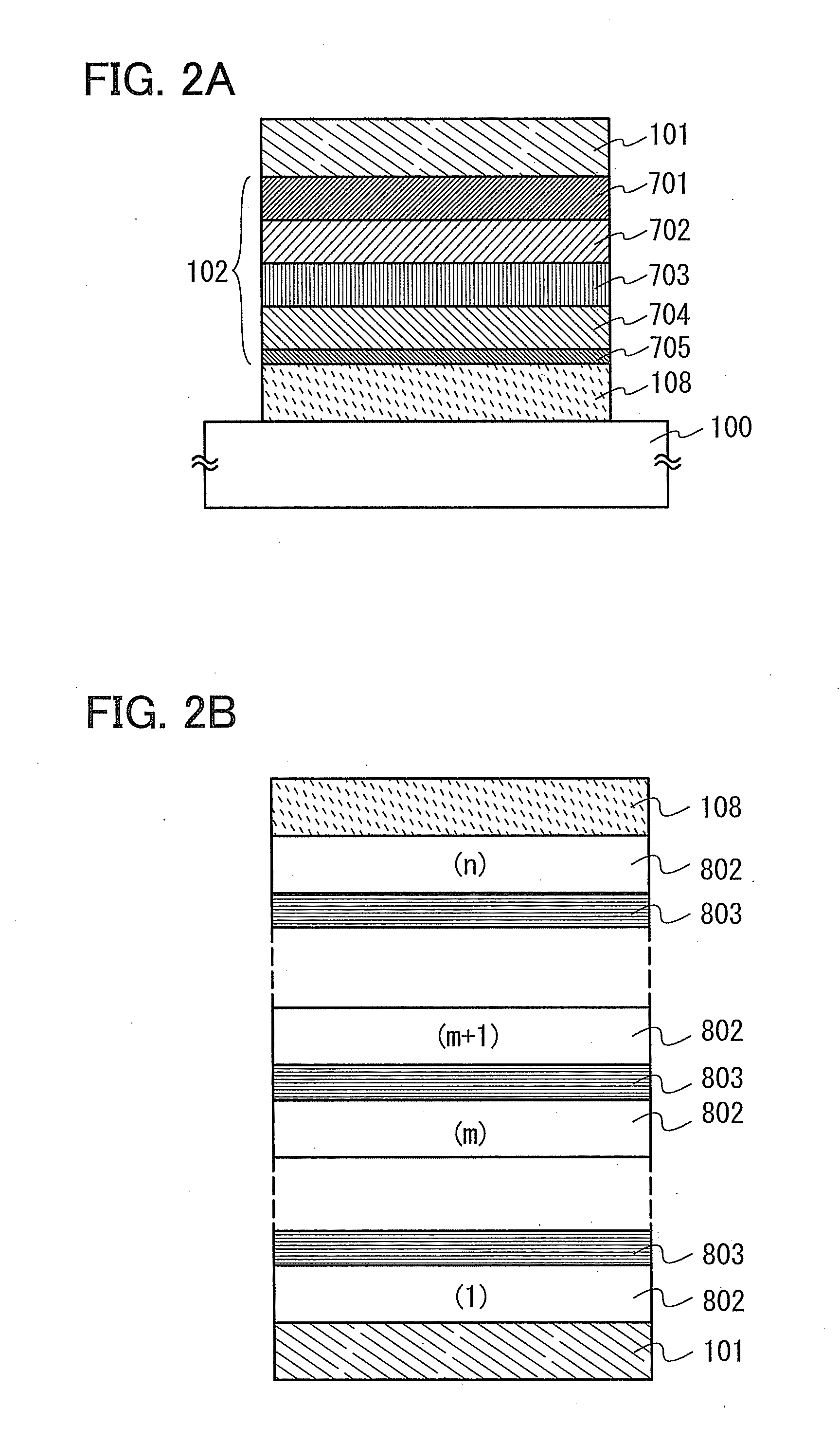
[0128]In this embodiment, a light-emitting element of one embodiment of the present invention will be described with reference to FIGS. 1A to 1C.

[0129]In a light-emitting element of this embodiment, an EL layer (a layer containing a light-emitting substance) is interposed between a pair of electrodes. The EL layer includes at least a layer containing the composite material of one embodiment of the present invention described in Embodiment 1 and a light-emitting layer. The EL layer may additionally include another layer. For example, the EL layer may include a layer containing a substance having a high carrier-injection property or a layer containing a substance having a high carrier-transport property so that a light-emitting region is fowled in a region away from the electrodes, that is, so that carriers recombine in a region away from the electrodes. In this specification, the layer containing a substance having a high carrier-injection or a high carrier-transport property is also...

embodiment 3

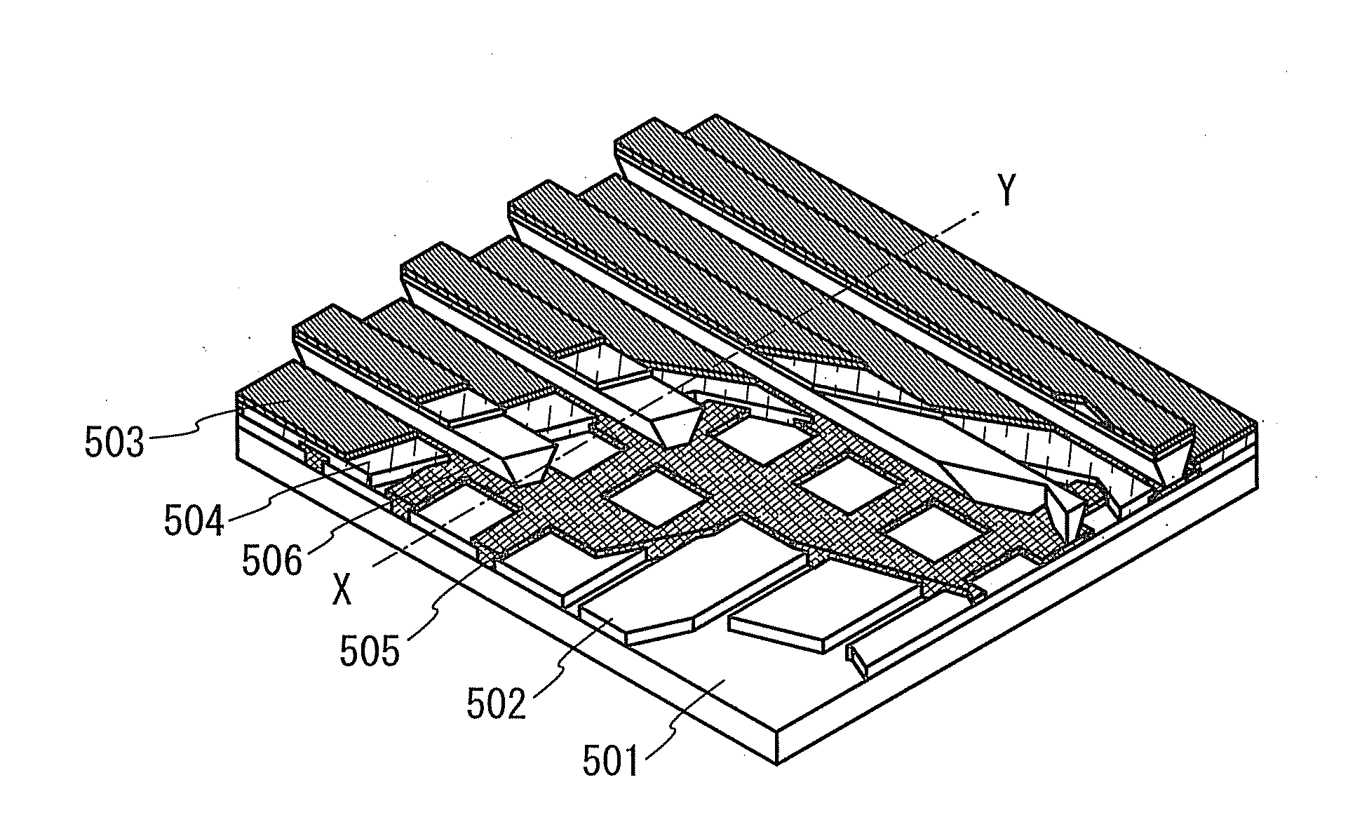
[0184]In this embodiment, a light-emitting device including a light-emitting element of one embodiment of the present invention will be described with reference to FIGS. 3A and 3B. Note that FIG. 3A is a top view illustrating the light-emitting device, and FIG. 3B is a cross-sectional view taken along lines A-B and C-D of FIG. 3A.

[0185]In FIG. 3A, reference numeral 401 denotes a driver circuit portion (a source side driver circuit), reference numeral 402 denotes a pixel portion, and reference numeral 403 denotes a driver circuit portion (a gate side driver circuit), which are each indicated by dotted lines. Reference numeral 404 denotes a sealing substrate, reference numeral 405 denotes a sealing material, and a portion enclosed by the sealing material 405 is a space 407.

[0186]Note that a lead wiring 408 is a wiring for transmitting signals that are to be input to the source side driver circuit 401 and the gate side driver circuit 403, and receives a video signal, a clock signal, a ...


PUM


Abstract

A composite material including an organic compound and an inorganic compound and having a high carrier-transport property is provided. A composite material having a high carrier-injection property to an organic compound is provided. A composite material in which light absorption due to charge transfer interaction is unlikely to occur is provided. A light-emitting element having high emission efficiency is provided by including the composite material. A light-emitting element having a low drive voltage is provided. A light-emitting element having a long lifetime is provided. A composite material including a heterocyclic compound having a dibenzothiophene skeleton or a dibenzofuran skeleton and an inorganic compound exhibiting an electron-accepting property with respect to the heterocyclic compound is provided.

Description

TECHNICAL FIELD[0001]The present invention relates to a composite material including an organic compound and an inorganic compound, a light-emitting element, a light-emitting device, an electronic device, and a lighting device.BACKGROUND ART[0002]In recent years, research and development have been extensively conducted on light-emitting elements using organic electroluminescence (EL). In a basic structure of such a light-emitting element, a layer containing a light-emitting organic compound is interposed between a pair of electrodes. By applying voltage to this element, light emission from the light-emitting organic compound can be obtained.[0003]Since such a light-emitting element is of self-light-emitting type, it is considered that the light-emitting element has advantages over a liquid crystal display in that visibility of pixels is high, backlight is not required, and so on and is therefore suitable as flat panel display elements. In addition, it is also a great advantage that ...

Claims


Application Information

Patent Timeline
IPC IPC(8): H01L51/54C09K11/06
CPCC09K11/06C09K2211/1007C09K2211/1011C09K2211/1088C09K2211/1092H05B33/14H01L51/0072H01L51/0073H01L51/0074H01L51/5048H01L2251/303H01L51/0052H10K85/615H10K85/6576H10K85/6574H10K85/6572H10K50/14H10K2102/00H10K85/657H10K50/13H10K50/11H10K50/00
Inventor NOWATARI, HIROMISEO, SATOSHIOSAKA, HARUETAKASU, TAKAKO
Owner SEMICON ENERGY LAB CO LTD
Why Eureka
Try Eureka