Metal Interconnection Structure and Method For Forming Metal Interlayer Via and Metal Interconnection Line

a metal interconnection and metal layer technology, applied in the field of metal interconnection structure and methods for forming metal interlayer vias and metal interconnection lines, can solve the problems of more and more difficult to fill contact holes, failure of devices, and more and more difficult to fill the second barrier layer b>32/b> and the first copper layer, so as to reduce the difficulty in filling the second metal layer

Active Publication Date: 2012-04-05
INST OF MICROELECTRONICS CHINESE ACAD OF SCI
View PDF8 Cites 38 Cited by
  • Summary
  • Abstract
  • Description
  • Claims
  • Application Information

AI Technical Summary

Benefits of technology

[0017]The seed layer is formed on the first dielectric layer and the first metal layer before the second metal layer is formed, so that the mask pattern is formed on the seed layer. As a result, in forming the second metal layer by using the mask pattern, the second metal layer is formed from the bottom upward on the portion of the seed layer exposed by the mask patter. Unlike the prior art, the seed layer no longer covers any corner of the exposed region. Thus, it is possible to reduce the possibility that the neck blocking effect occurs at the corner and the possibility that voids occur in forming the second metal layer in the exposed region. Further, since the seed layer is formed on the first dielectric layer and the first metal layer, that is, the seed layer is formed on the surface defined by the first dielectric layer and the first metal layer, the second metal layer is grown from the bottom upward in the plating process, and there is no need for the seed layer on the side walls. Thus, it is possible to reduce the difficulty in filling the second metal layer due to the poor coverage of the seed layer on the side walls and the neck blocking effect as described above. As a result,

Problems solved by technology

As a result, it is more and more difficult to fill the contact hole, the first trench 50, the further trenches and the through hole to form a metal interconnection structure satisfying the process requirements.
A common problem is that in filling the contact hole, the through hole, and the first trench 50 and the further trenches with copper to form the contact plug, the interlayer via and the metal interconnection lines, voids may be generated in the contact plug, the via or the metal interconnection lines, which tend to cause failure of devices.
Furthermore, with the continuously increasing of the depth-to-width ratio of the trench, it is more and more difficult for the second barrier l

Method used


Image

  • Metal Interconnection Structure and Method For Forming Metal Interlayer Via and Metal Interconnection Line
  • Metal Interconnection Structure and Method For Forming Metal Interlayer Via and Metal Interconnection Line
  • Metal Interconnection Structure and Method For Forming Metal Interlayer Via and Metal Interconnection Line

Examples


Embodiment Construction

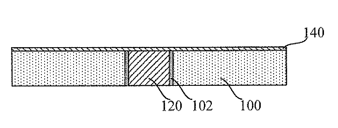
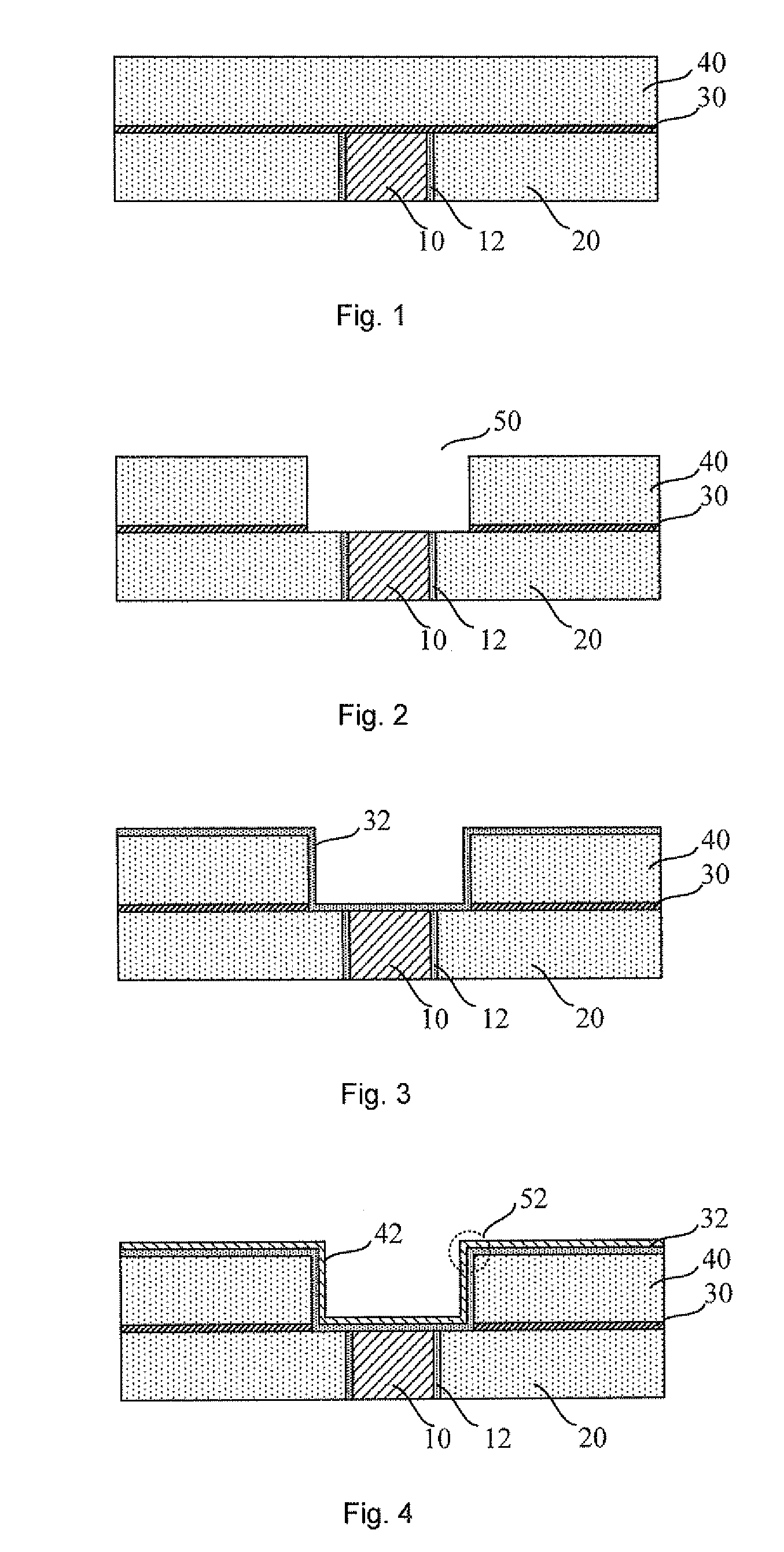
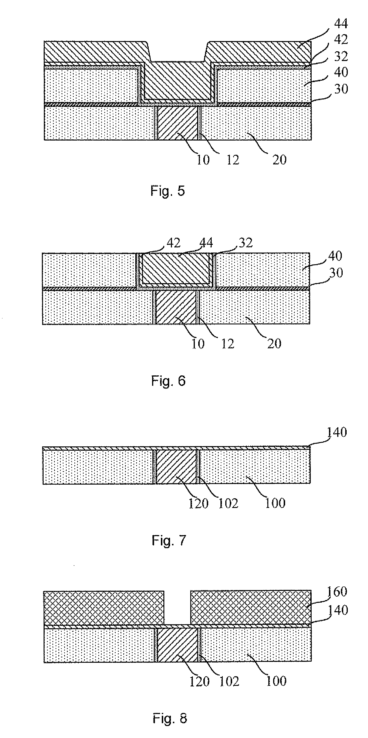
[0024]The disclosure hereinafter provides various embodiments or examples to explain the concept of the present invention. Though specific exemplary parts and arrangements are described in the following, they are just examples and not intended to limit the present invention.

[0025]Further, in this disclosure same reference numerals and / or symbols may be repeated through different embodiments. Such repeating is for the purpose of simplification and clarity, and does not indicate relationships between the various embodiments and / or arrangements discussed here.

[0026]In this disclosure, examples for various specific processes and / or materials are provided. However, substitution of other processes and / or other materials which are apparent for those skilled in the art does not depart from the scope of the present invention. It is to be noted that boundaries of various regions described in this disclosure include necessary extensions required by the processes.

[0027]According to the present ...


PUM


Abstract

There is provided a method for forming a metal interlayer via, comprising: forming a seed layer on a first dielectric layer and a first metal layer embedded in the first dielectric layer; forming a mask pattern on the seed layer to expose a portion of the seed layer covering some of the first metal layer; growing a second metal layer on the exposed portion of the seed layer; removing the mask pattern and a portion of the seed layer carrying the mask pattern to expose side walls of the second metal layer, a portion of the first metal layer and the first dielectric layer; forming an insulating barrier layer on the side walls, the portion of the first metal layer and the first dielectric layer. There is also provided a method for forming a metal interconnection line. Both of them can suppress the occurrence of voids. There is further provided a metal interconnection structure comprising a contact plug, a via and a metal interconnection line, wherein the via is formed on the metal interconnection line, the metal gate and/or the contact plug.

Description

FIELD OF INVENTION[0001]The present invention relates to the semiconductor field, and more particularly, to a metal interconnection structure and methods for forming a metal interlayer via and a metal interconnection line.BACKGROUND[0002]In practice, a metal interconnection structure is usually formed by Damascene process in the semiconductor industry, including forming a metal interconnection line on a contact plug, forming an interlayer via on the metal interconnection line and then forming an upper-layer metal interconnection line on the interlayer via. The process can be repeated several times to achieve an interconnection of multiple metal layers.[0003]The first metal interconnection line (M1) is implemented by Single Damascene process. Specifically, first, as shown in FIG. 1, on a first dielectric layer 20 and a first metal layer 10 (generally referred to as a contact plug) embedded in the first dielectric layer 20, a first barrier layer 30 and a second dielectric layer 40 are...

Claims


Application Information

Patent Timeline
IPC IPC(8): H01L23/52H01L21/768
CPCH01L21/76834H01L21/76873H01L23/53295H01L23/53238H01L23/5329H01L21/76885H01L2924/0002H01L2924/00
Inventor ZHAO, CHAO
Owner INST OF MICROELECTRONICS CHINESE ACAD OF SCI
Why Eureka
Try Eureka