Semiconductor device production method and semiconductor production apparatus

a semiconductor and production method technology, applied in the direction of electrolysis process, electrolysis components, cells, etc., can solve the problems of difficult to fill a metal in the wiring region, difficult in the prior art electroplating method and electroplating apparatus to measure, and difficult to create any voids

Inactive Publication Date: 2009-09-17
PANASONIC CORP
View PDF9 Cites 0 Cited by
  • Summary
  • Abstract
  • Description
  • Claims
  • Application Information

AI Technical Summary

Benefits of technology

[0010]It is difficult in the prior art electroplating method and electroplating apparatus to measure and assess the concentration of all constituents present in the plating solution including by-products produced in the course of plating. Therefore, it is difficult to fill a metal in the wiring regions consisting of nanoscale microstructures in semiconductor devices without creating any voids.

Problems solved by technology

It is difficult in the prior art electroplating method and electroplating apparatus to measure and assess the concentration of all constituents present in the plating solution including by-products produced in the course of plating.
Therefore, it is difficult to fill a metal in the wiring regions consisting of nanoscale microstructures in semiconductor devices without creating any voids.

Method used


Image

  • Semiconductor device production method and semiconductor production apparatus
  • Semiconductor device production method and semiconductor production apparatus
  • Semiconductor device production method and semiconductor production apparatus

Examples


first embodiment

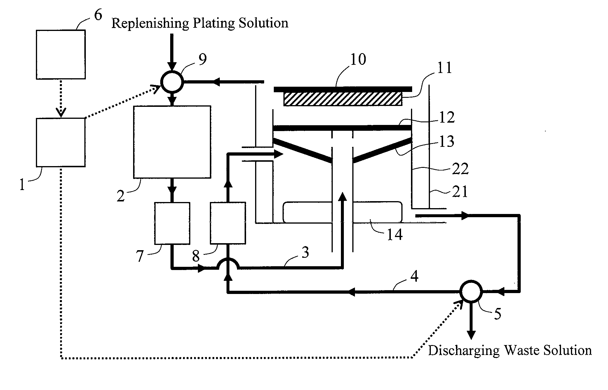
[0028]A first embodiment of the present invention is described hereafter with reference to FIG. 1.

[0029]FIG. 1 is a schematic diagram showing the structure of an electroplating apparatus relating to the first embodiment. The electroplating apparatus comprises a plating chamber 21 having a partition 22. An anode 14 is placed at the bottom of the plating chamber 21. Facing the anode 14, a cathode 10 holds a wafer 11 in a manner such that the surface to be treated is oriented toward the anode 14. A filter 13 and a diffusion plate 12 are provided between the anode 14 and cathode 10 in this order from the anode 14. The electroplating apparatus of this embodiment further comprises a circulation line 3 and a sub-circulation line 4 as the plating solution circulation path. The circulation line 3 is a circulation path allowing the plating solution from the top end of the plating chamber 21 to re-enter between the diffusion plate 12 and filter 13 via a plating tank 2 and a filter 7. The sub-c...

second embodiment

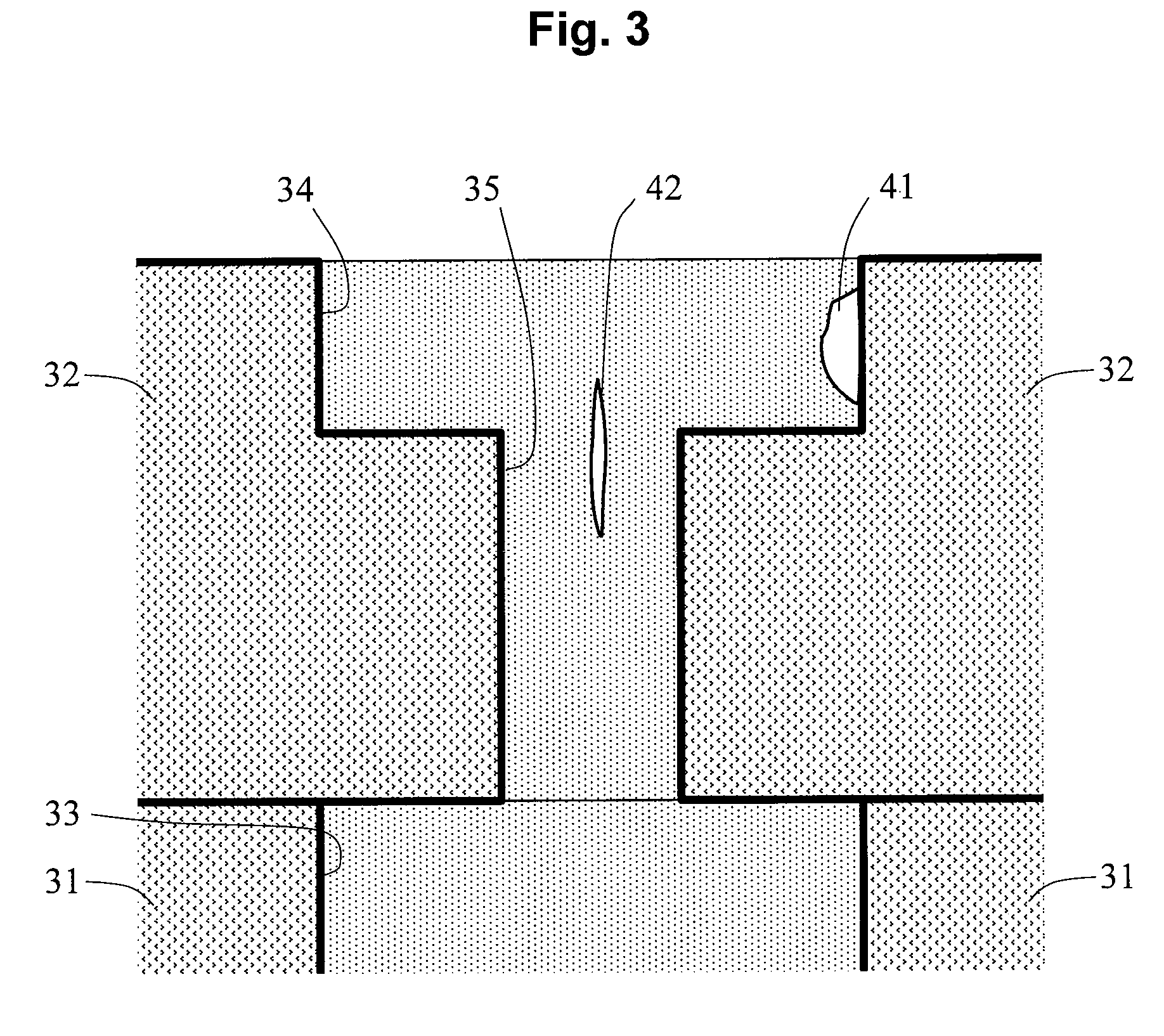
[0046]A second embodiment provides a filling method creating no defects such as voids and seams based on the first embodiment of the present invention.

[0047]FIG. 6 is a flowchart of a plating process presenting the second embodiment. When the electroplating apparatus starts a recipe for plating, first, the monitoring unit 6 measures the concentrations of the three additives (S1). The monitoring unit 6 orders the control unit 1 to replenish plating solution in the case of NG in which the measurements are outside predetermined value ranges. The control unit 1 being ordered opens the supply valve 9 and replenishes a predetermined volume of plating solution (S1NG, S2). When the replenishment is completed, the monitoring unit 6 measures the concentrations of the additives once again (S1). The replenishment of plating solution is repeated until the concentrations of the additives are within the above predetermined ranges. When the replenished volume exceeds the total volume of plating sol...

third embodiment

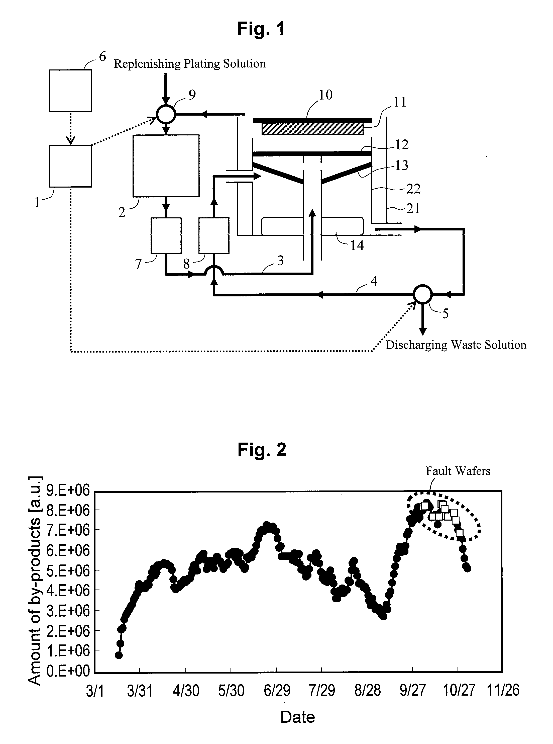
[0050]A third embodiment of the present invention will be described hereafter. The third embodiment of the present invention relates to an electroplating method in which the optimum volume of waste solution is determined. The plating solution is expensive and it is preferable that the volume of waste solution is minimized. Then, in this embodiment, a technique of determining the optimum volume of waste solution based on the quantity of wafers to be processed, namely the amount of by-products to be produced, total volume of plating solution, and volume of waste solution, will be described.

[0051]FIG. 7 is a graphical representation showing results of simulating the amount of by-products in the plating solution in relation to the number of times of discharging waste solution. Here, the amounts of by-products were calculated for the cases when volume ratios of waste solution to the total volume of plating solution (hereafter, referred to as a waste solution ratio) were 8% and 29% with t...


PUM

PropertyMeasurementUnit
currentaaaaaaaaaa
volumeaaaaaaaaaa
diameteraaaaaaaaaa

Abstract

A semiconductor device production method of the present invention first collects data including an initial volume of plating solution, volume of replenished solution, number of wafers processed, value of current applied and volume of waste solution in a step of filling a metal plating film in a via hole or a trench formed in an insulating film on a semiconductor substrate. Then, a cumulative charge during the plating is calculated based on the obtained current value. Also, a total volume of plating solution is calculated. Furthermore, an amount of decomposition products of suppressors contained in the plating solution based on the calculated total volume of plating solution, the volume of waste solution and the calculated cumulative charge. The semiconductor substrate is plated only when the amount of decomposition products is equal to or smaller than a predetermined threshold.

Description

CROSS-REFERENCE TO RELATED APPLICATION[0001]The present application claims the benefit of Japanese Patent Application No. 2008-060835 filed Mar. 11, 2008, the subject matter of which is incorporated herein by reference.BACKGROUND OF THE INVENTION[0002]1. Field of the Invention[0003]The present invention relates to a semiconductor device production method and a semiconductor production apparatus and particularly to a plating method and a plating apparatus used in a metal wiring process for semiconductor devices.[0004]2. Description of the Related Art[0005]FIG. 9 is a schematic diagram showing a structure of a prior art electroplating apparatus. This electroplating apparatus comprises a circulation line 101, a plating tank 102, a cathode 104, an anode 105, a wafer 106, a filter 107, an additive concentration measurement unit 108, a CPU 109, and an additive supply unit 110.[0006]In prior art electroplating, metal-plating is performed while additives are supplied (reference is made, for...

Claims


Application Information

Patent Timeline
Patent Type & Authority Applications(United States)
IPC IPC(8): C25D21/12C25D17/00
CPCC25D21/12C25D21/18C25D17/001H01L21/76877H01L21/2885
Inventor IMAI, SHIN-ICHITANAKA, TOMOYAKITABATA, MASAKAI
Owner PANASONIC CORP
Why Eureka
Try Eureka