Semiconductor device, and method of diagnosing abnormality of boosting circuit of semiconductor device

a technology of semiconductor devices and boosting circuits, which is applied in the direction of pulse manipulation, pulse technique, transportation and packaging, etc., can solve the problems of deterioration in the accuracy of measuring battery voltage by the output voltage vou

Active Publication Date: 2012-04-05
LAPIS SEMICON CO LTD
View PDF1 Cites 19 Cited by
  • Summary
  • Abstract
  • Description
  • Claims
  • Application Information

AI Technical Summary

Benefits of technology

[0010]Here, in the case of measuring the voltage of the battery cell Vc5, when the power supply voltage VCC is not boosted by the boosting circuit 42 and is supplied as is to the buffer amplifier 130, the buffer imp 132 of the buffer amplifier 120, at the buffer amplifier 130, Vx=V5=VCC, and the input voltage and the power supply voltage (driving voltage) become the same, and the transistor within the buffer amplifier 130 operates in a non-saturated region, and offset voltage Vos of output Vx1 of the buffer amplifier 130 becomes large. As a result, there are cases in which the accuracy of measuring the battery voltage by the output voltage Vout deteriorates. Therefore, in the semiconductor device 100, the power supply voltage VCC is boosted by the boosting circuit 142 to the driving voltage VCC1 that can make the transistor within the buffer amplifier 130 operate in the saturated region, and the driving voltage VCC1 is supplied to the buffer amplifier 130. Due thereto, the offset voltage Vos of the buffer amplifier 130 is suppressed, and the accuracy of measuring the battery voltage by the output voltage Vout is improved.
[0024]In accordance with the present invention, there is the effect that an abnormality of a boosting circuit provided at a semiconductor device can be diagnosed.

Problems solved by technology

As a result, there are cases in which the accuracy of measuring the battery voltage by the output voltage Vout deteriorates.

Method used


Image

  • Semiconductor device, and method of diagnosing abnormality of boosting circuit of semiconductor device
  • Semiconductor device, and method of diagnosing abnormality of boosting circuit of semiconductor device
  • Semiconductor device, and method of diagnosing abnormality of boosting circuit of semiconductor device

Examples


Embodiment Construction

[0032]A semiconductor device for battery monitoring of the present exemplary embodiment is described in detail hereinafter with reference to the drawings.

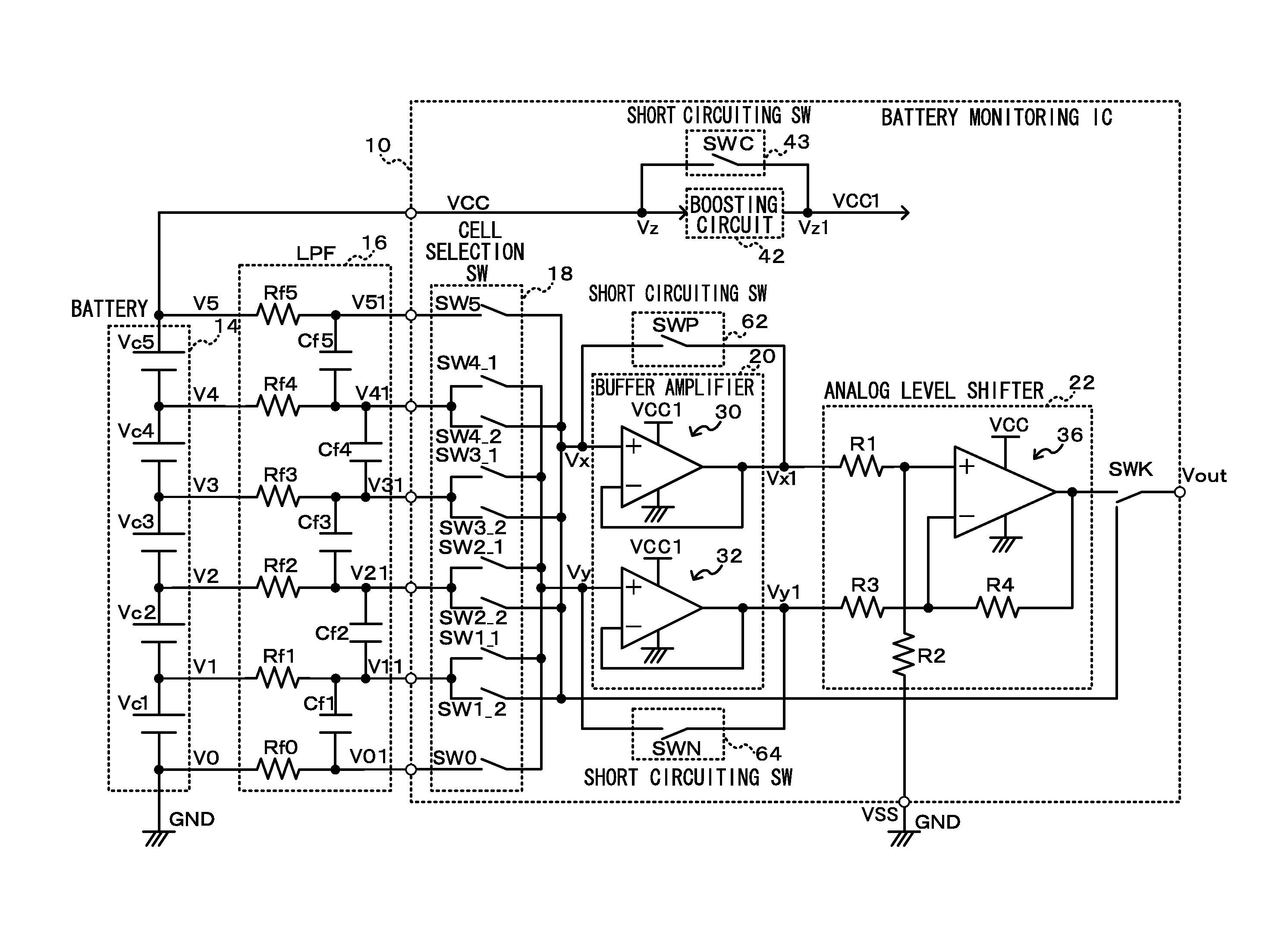
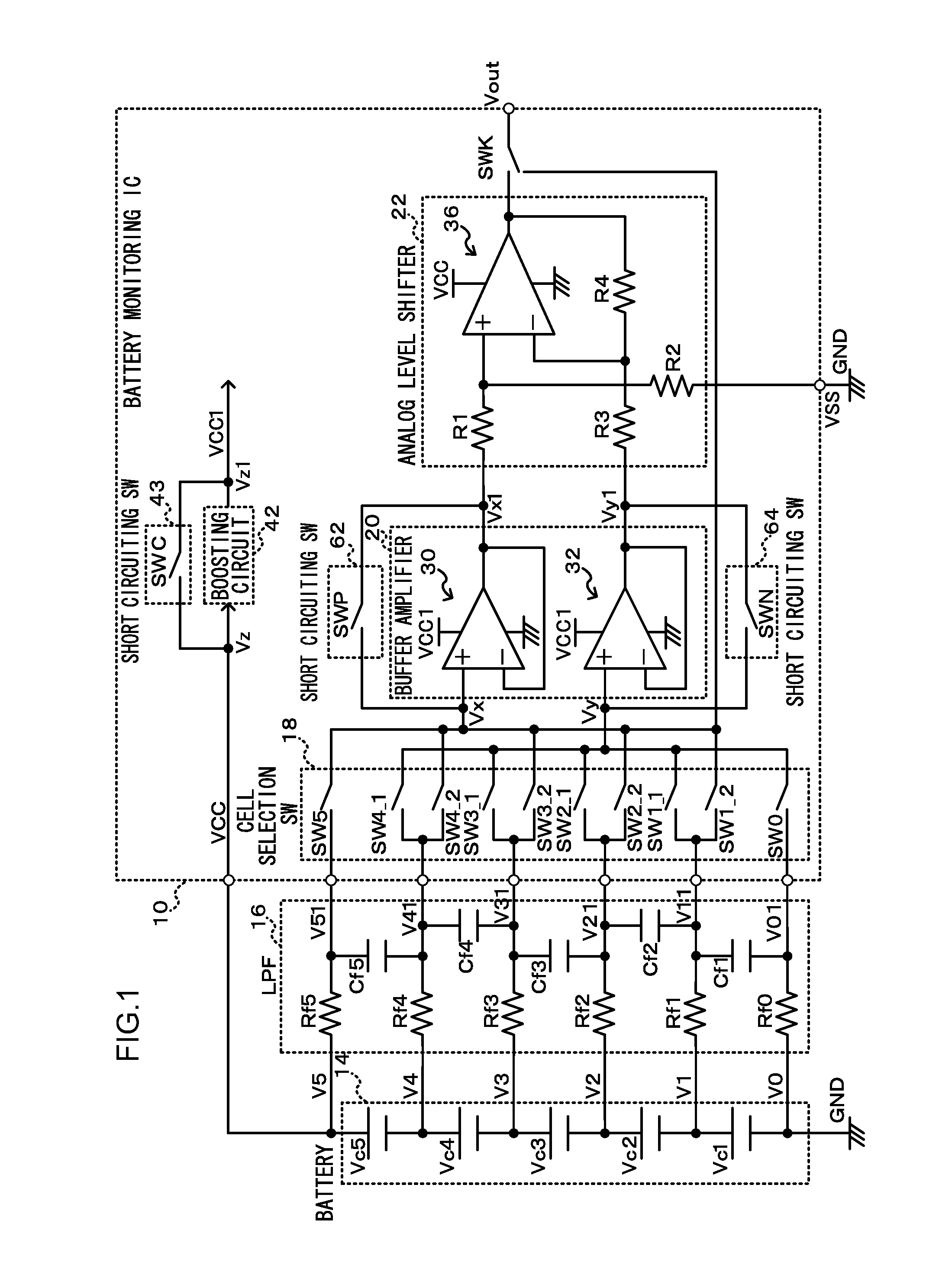
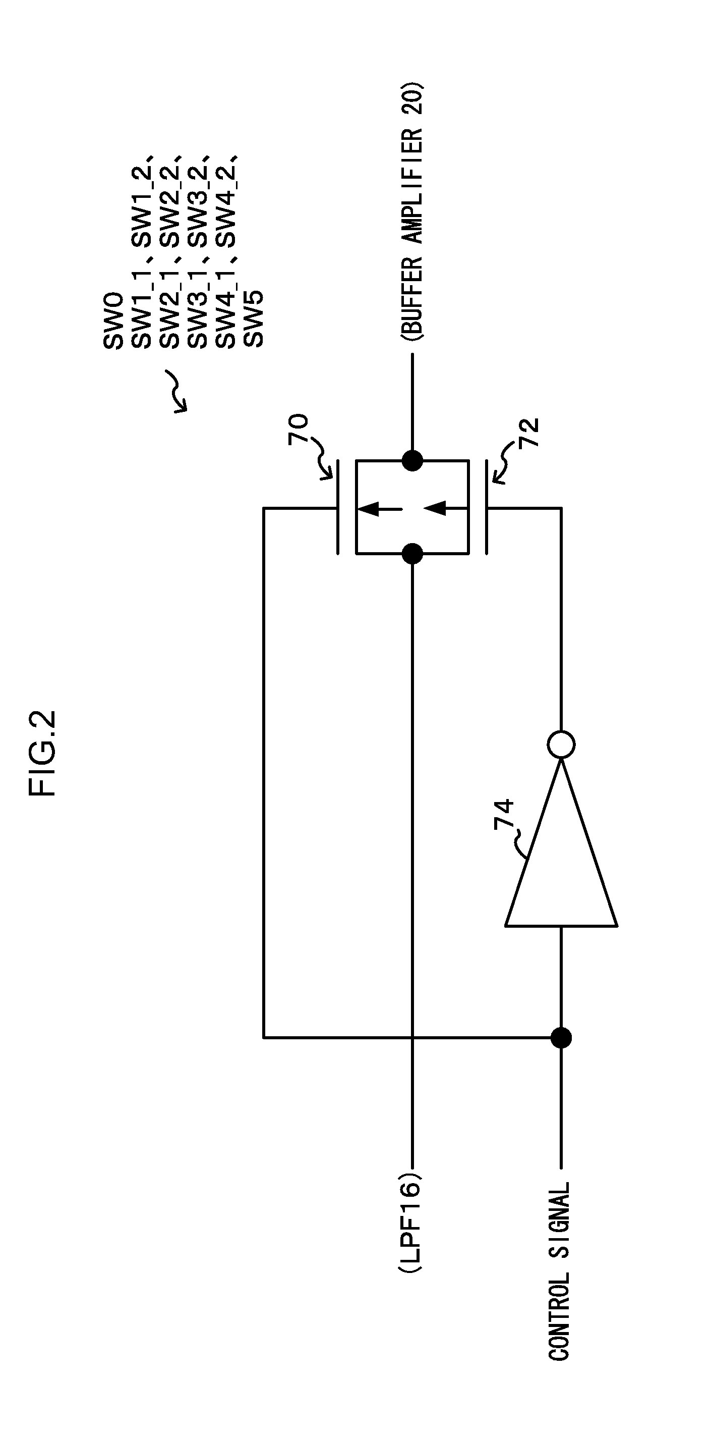
[0033]A circuit diagram of an example of the schematic structure of a semiconductor device (battery monitoring IC) of the present exemplary embodiment is shown in FIG. 1. A battery monitoring IC 10 of the present exemplary embodiment is structured to have a cell selection SW 18, a buffer amplifier 20, and an analog level shifter 22. The buffer amplifier 20 is structured to include a buffer amplifier 30, a buffer amplifier 32, a boosting circuit 42, and a short circuiting SW 43 that is used at the time of diagnosing an abnormality of the boosting circuit 42. The analog level shifter 22 structures a differential amplification circuit from detection resistors R1, R2, R3, R4 and an amplifier 36.

[0034]A battery 14 includes five battery cells Vc1 through Vc5 that are connected in series, and the negative electrode of the battery cell Vc1...


PUM


Abstract

The battery monitoring IC is provided with the short circuiting switch that includes the switching element that shorts the input side and the output side of the boosting circuit that boosts the power supply voltage to the driving voltage, that can drive the MOS transistor within the buffer amplifier in the saturated region, and supplies the driving voltage as the driving voltage of the buffer amplifier. An abnormality of the boosting circuit can be diagnosed by comparing the output voltage, that is measured when the short circuiting switch is turned off and the driving voltage boosted by the boosting circuit is supplied to the buffer amplifier, and the output voltage, that is measured when the short circuiting switch is turned on and the power supply voltage is, without going through the boosting circuit, supplied as is to the buffer amplifier.

Description

CROSS-REFERENCE TO RELATED APPLICATION[0001]This application is based on and claims priority under 35 USC 119 from Japanese Patent Application No. 2010-221807 filed on Sep. 30, 2010, the disclosure of which is incorporated by reference herein.BACKGROUND[0002]1. Technical Field[0003]The present invention relates to a semiconductor device and a method of diagnosing a boosting circuit of a semiconductor device, and in particular, relates to a semiconductor device for battery monitoring and a method of diagnosing an abnormality of a boosting circuit of a semiconductor device for battery monitoring.[0004]2. Related Art[0005]Generally, there are semiconductor devices for carrying out monitoring and control of plural batteries that are connected in series. A battery monitoring IC (Integral Circuit) for monitoring and controlling a battery that is installed in a vehicle or the like for example, is known as such a semiconductor device for battery monitoring.SUMMARY[0006]The semiconductor dev...

Claims


Application Information

Patent Timeline
Patent Type & Authority Applications(United States)
IPC IPC(8): H03L5/00
CPCY02T10/7055H02J7/0021Y02T10/70H02J7/0013H02J7/0048H02J7/005
Inventor BAN, MASAFUMI
Owner LAPIS SEMICON CO LTD
Why Eureka
Try Eureka