
Display Device And Method For Driving Same

a liquid crystal display and display device technology, applied in the field of display devices, can solve the problems of abnormal operation or inoperableness, increase in the amount of heat generated in the source driver lsi, and increase in the amount of power required to drive the panel of the liquid crystal display device, so as to achieve the effect of reducing the amplitude of the applied voltage to the video signal line, and increasing the voltage difference between the subpixels

Inactive Publication Date: 2012-04-12
SHARP KK
View PDF0 Cites 9 Cited by
  • Summary
  • Abstract
  • Description
  • Claims
  • Application Information

AI Technical Summary

Benefits of technology

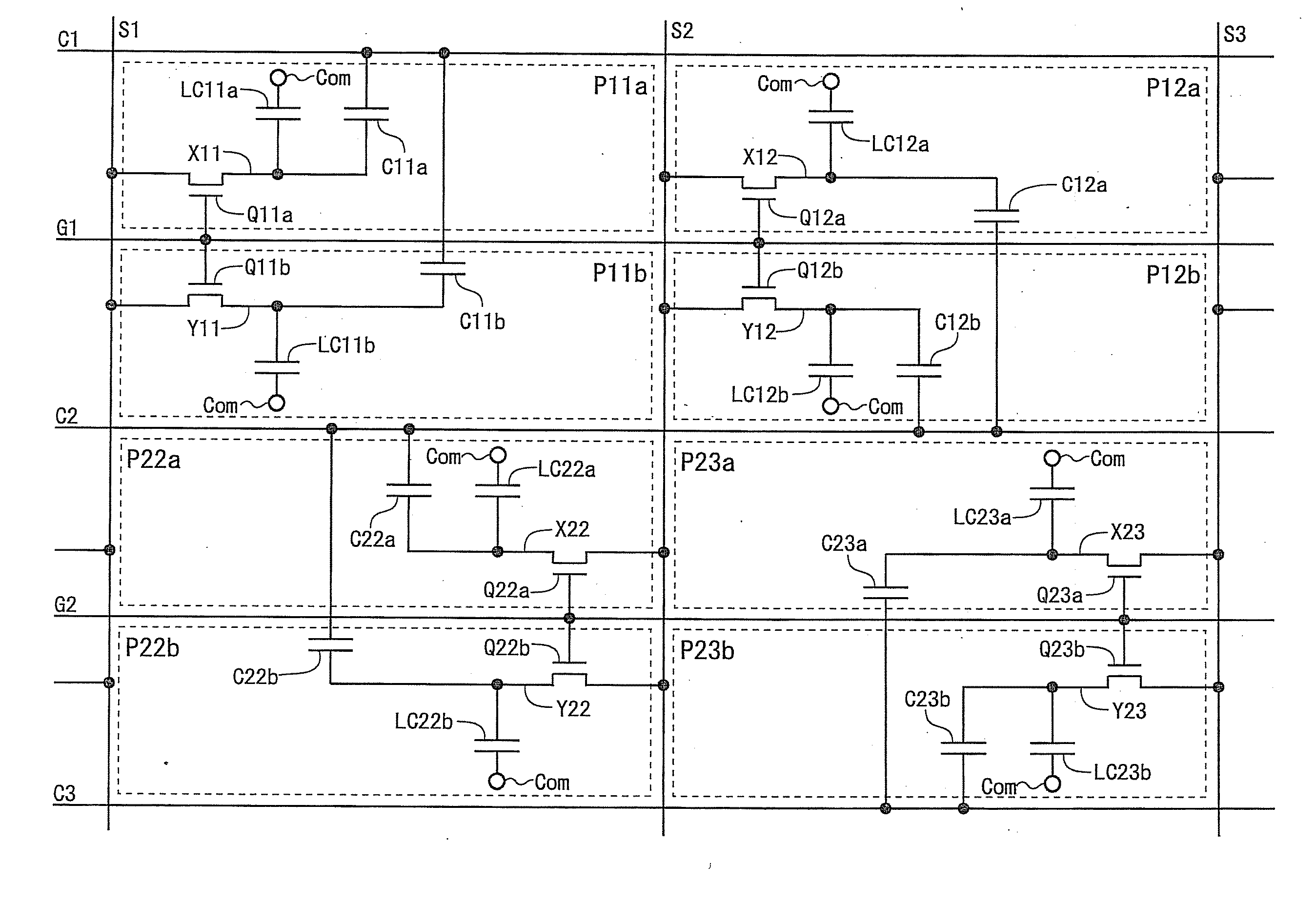
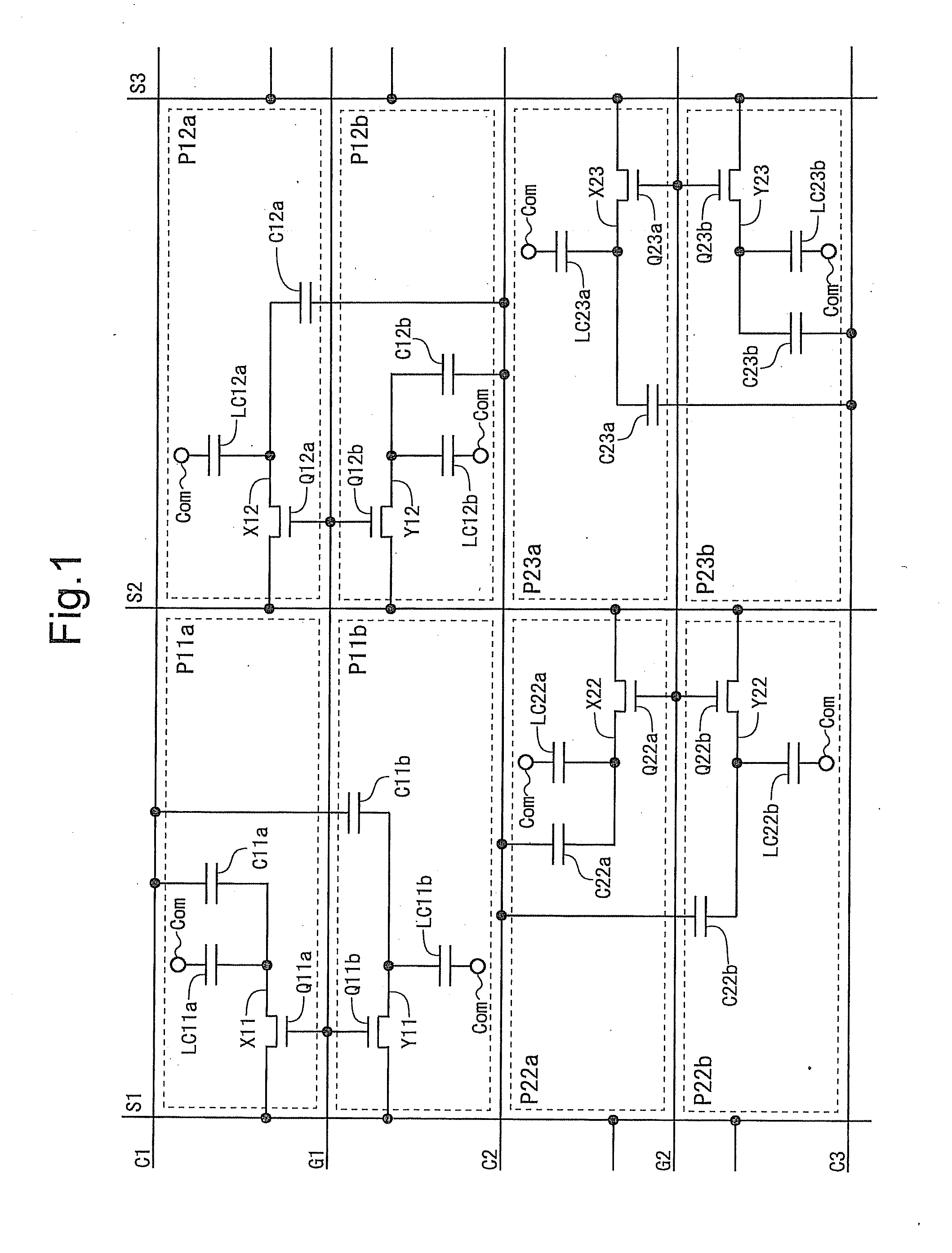
[0059]According to the first aspect of the present invention, a pixel formation portion is composed of a first subpixel portion and a second subpixel portion. By a pixel electrode voltage shift portion changing an applied voltage to an auxiliary capacitance wiring line, the voltages of pixel electrodes in the two subpixel portions change. Hence, the amplitudes of the voltages of the pixel electrodes become greater than the amplitude of a voltage provided to a video signal line. By this, the amplitude of the applied voltage to the video signal line can be reduced over conventional cases. In addition, by changing the voltage of the pixel electrode in each subpixel portion by the pixel electrode voltage shift portion, an effective voltage of a first pixel electrode (the pixel electrode in the first subpixel portion) is made different in magnitude from an effective voltage of a second pixel electrode (the pixel electrode in the second subpixel portion). From the above, a display device is implemented in which even if the amplitude of an applied voltage to a video signal line is relatively small, the amplitudes of the voltages of subpixels can be increased and the voltage difference between the subpixels can be furthermore increased.
[0060]According to the second aspect of the present invention, as with the first aspect of the present invention, a display device is implemented in which even if the amplitude of an applied voltage to a video signal line is relatively small, the amplitudes of the voltages of subpixels can be increased and the voltage difference between the subpixels can be furthermore increased.
[0061]According to the third aspect of the present invention, the level of the influence exerted by a change in the applied voltage to the auxiliary capacitance wiring line can be made different between the first pixel electrode and the second pixel electrode. By this, a voltage difference can be generated between subpixels, with a simple configuration.
[0062]According to the fourth aspect of the present invention, when dot-reversal driving is adopted, there is no need to reverse the polarity of an applied voltage to each video signal line every horizontal scanning period and thus the polarities of applied voltages to each video signal line are made to be the same throughout one frame period. Hence, since the number of times the video signal lines are charged and discharged is reduced, power consumption is reduced and an increase in the amount of heat generated in a video signal line driving LSI is suppressed.
[0063]According to the fifth aspect of the present invention, in a configuration in which active elements in two subpixel portions are controlled by scanning signals from different scanning signal lines, the level of the influence exerted by a change in the applied voltage to the auxiliary capacitance wiring line can be made different between the first pixel electrode and the second pixel electrode.
[0064]According to the sixth aspect of the present invention, as with the fifth aspect of the present invention, in a configuration in which active elements in two subpixel portions are controlled by scanning signals from different scanning signal lines, the level of the influence exerted by a change in the applied voltage to the auxiliary capacitance wiring line can be made different between the first pixel electrode and the second pixel electrode.

Problems solved by technology

As a result, there has been a noticeable increase in the amount of power required to drive the panel of a liquid crystal display device.
In addition, in recent years, there has also been a noticeable increase in the amount of heat generated in a source driver LSI.
If the temperature of the source driver LSI exceeds an acceptable range of temperatures as a result of the increase in the amount of heat generated, then the source driver LSI may cause abnormal operation or become inoperable.

Method used


Image

  • Display Device And Method For Driving Same
  • Display Device And Method For Driving Same
  • Display Device And Method For Driving Same

Examples


first embodiment

1. First Embodiment

[0091]

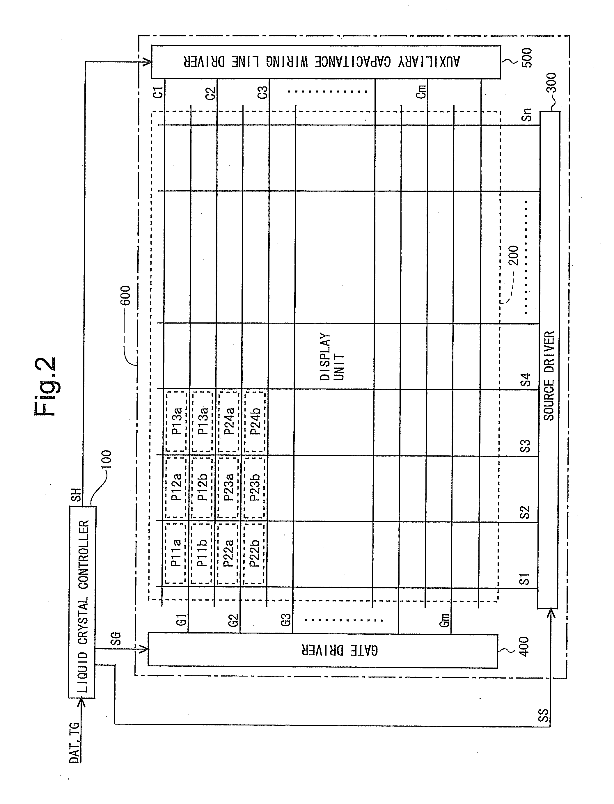
[0092]FIG. 2 is a block diagram showing an overall configuration of a liquid crystal display device according to a first embodiment of the present invention. The liquid crystal display device is composed of a liquid crystal panel 600 and a liquid crystal controller 100. The liquid crystal panel 600 includes a display unit 200, a source driver (video signal line drive circuit) 300, a gate driver (scanning signal line drive circuit) 400, and an auxiliary capacitance wiring line driver (auxiliary capacitance wiring line drive circuit) 500. Note that in FIG. 2 a polarizing plate and a backlight which are disposed on the front and back sides of the liquid crystal panel 600 are omitted. Also, it is assumed that the liquid crystal display device performs 256-level grayscale display.

[0093]The display unit 200 includes n source wiring lines (video signal lines) S1 to Sn, m gate wiring lines (scanning signal lines) G1 to Gm, and a plurality of (n×m) pixel formation po...

second embodiment

2. Second Embodiment

[0114]

[0115]FIG. 6 is a block diagram showing an overall configuration of a liquid crystal display device according to a second embodiment of the present invention. The liquid crystal display device is composed of a liquid crystal panel 600 and a liquid crystal controller 100. The liquid crystal panel 600 includes a display unit 200, a source driver (video signal line drive, circuit) 300, a gate driver (scanning signal line drive circuit) 400, and an auxiliary capacitance wiring line driver (auxiliary capacitance wiring line drive circuit) 500. Note that in FIG. 6 a polarizing plate and a backlight which are disposed on the front and back sides of the liquid crystal panel 600 are omitted. Also, it is assumed that the liquid crystal display device performs 256-level grayscale display. The operation of each component is the same as that in the above-described first embodiment and thus description thereof is omitted.

[0116]

[0117]FIG. 7 is a circuit diagram showing th...

third embodiment

3. Third Embodiment

[0136]

[0137]FIG. 12 is a block diagram showing an overall configuration of a display device according to a third embodiment of the present invention. In the present embodiment, in addition to the components provided in the above-described first and second embodiments, a correction wiring line driver 700 is provided in a liquid crystal panel 600. The correction wiring line driver 700 drives correction wiring lines SA and SB shown in FIG. 12, based on a correction wiring line driving control signal SHO provided from a liquid crystal controller 100. The operations of those components other than the correction wiring line driver 700 are the same as those in the first embodiment and thus description thereof is omitted.

[0138]

[0139]FIG. 13 is a circuit diagram showing the configuration of pixel circuits in the present embodiment. As shown in FIG. 13, two subpixel formation portions Pija and Pijb are arranged at an intersection of a source wiring line Sj and a gate wiring...


PUM


Abstract

There is provided a display device in which even if the amplitude of the voltage of a source wiring line is relatively small, the amplitudes of the voltages of subpixels can be increased and the voltage difference between the subpixels can be furthermore increased. In at least one example embodiment, voltages of equal magnitudes are provided to pixel electrodes in a first subpixel portion and a second subpixel portion from a source wiring line. Thereafter, by changing an applied voltage to an auxiliary capacitance wiring line, voltages of different magnitudes are provided to the pixel electrodes in the first subpixel portion and the second subpixel portion. By this, a voltage difference is generated between the pixel electrode in the first subpixel portion and the pixel electrode in the second subpixel portion.

Description

TECHNICAL FIELD[0001]The present invention relates to a display device and more particularly to an active matrix-type liquid crystal display device using thin film transistors.BACKGROUND ART[0002]In recent years, an increase in the size and achievement of high definition of liquid crystal display devices have been promoted. In addition, in liquid crystal televisions, an increase in the rate of drive frequency which is called “double speed (120 Hz)”, “quad-speed (240 Hz)”, etc., has also been promoted. As a result, there has been a noticeable increase in the amount of power required to drive the panel of a liquid crystal display device. The causes of the increase in the amount of power include that: the source wiring line capacitance and gate wiring line capacitance in the liquid crystal panel increase as an increase in size is promoted; the number of wiring lines in the liquid crystal panel increases as achievement of high definition is promoted; the number of times the wiring lines...

Claims


Application Information

Patent Timeline
IPC IPC(8): G09G3/36G06F3/038
CPCG09G3/3659G09G2300/043G09G2300/0443G09G2300/0447G02F2001/134354G09G2300/0876G09G2330/021G02F1/134309G02F1/13624G09G2300/0847G02F1/134354
Inventor NUMAO, TAKAJI
Owner SHARP KK
Learn More