High-voltage ESD protection device

Active Publication Date: 2012-04-19
SHANGHAI HUAHONG GRACE SEMICON MFG CORP
View PDF4 Cites 22 Cited by
  • Summary
  • Abstract
  • Description
  • Claims
  • Application Information

AI Technical Summary

Benefits of technology

[0039]In the high-voltage ESD protection device of the present invention, the ESD current can he discharged through the switched-on one or more low-voltage PNP transistors or low-voltage PMOS transistors and the high-voltage silicon controlled rectifier. After the high-voltage ESD protection device of the present invention is switched on, the snapback sustaining voltage of the whole structure is determined by the sum of the snapback sustaining voltages of one or more low-voltage PNP transistors or low-voltage PMOS transistors and the high-voltage silicon controlled rectifier. As the minimum snapback sustaining volt

Problems solved by technology

on. Generally, the reverse breakdown voltage of the high-voltage N-well/high-voltage P-well junction is high. therefore, the application of this structure is greatly lim
ed on. Which leads to a low on-resistance, a large amplification and a low sustaining voltage after snapba

Method used


Image

  • High-voltage ESD protection device
  • High-voltage ESD protection device
  • High-voltage ESD protection device

Examples


embodiment 1

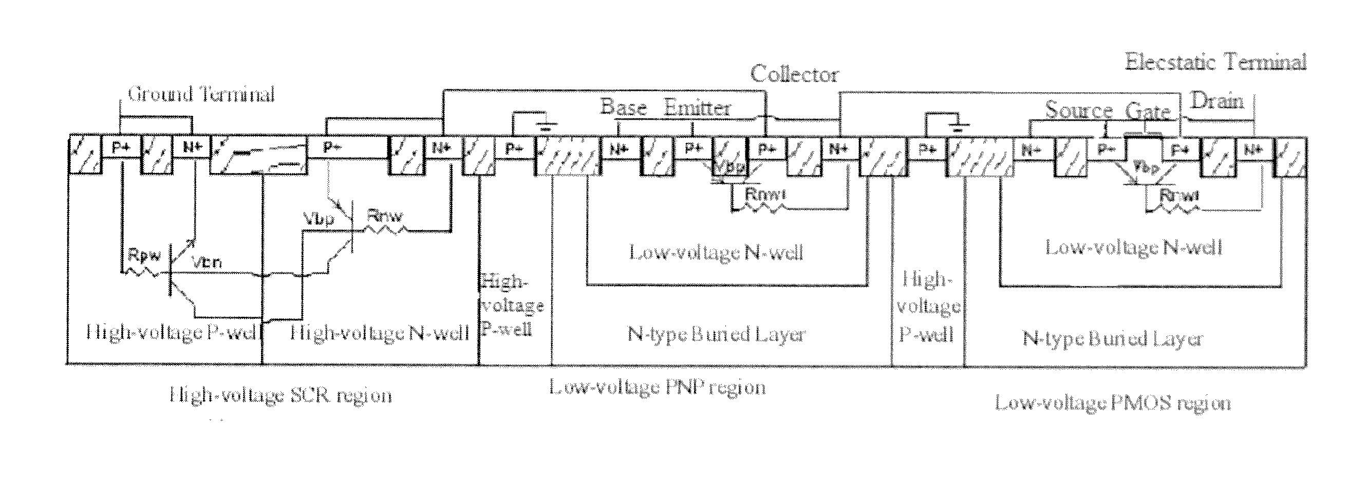
[0055]FIG. 3 shows the cross-sectional structure of a high-voltage ESD protection device in Embodiment 1 of the present invention. As shown in FIG. 3, the ESD protection device comprises a silicon controlled rectifier (SCR) and a first PNP transistor, wherein:

[0056]the silicon controlled rectifier and the first PNP transistor are formed on a P-type epitaxial layer of a silicon substrate and being adjacent to each other;

[0057]an isolation high-voltage P-well is formed on the P-type epitaxial layer of the silicon substrate between the silicon controlled rectifier and the first PNP transistor, the isolation high-voltage P-well isolates the silicon controlled rectifier from the first PMOS transistor;

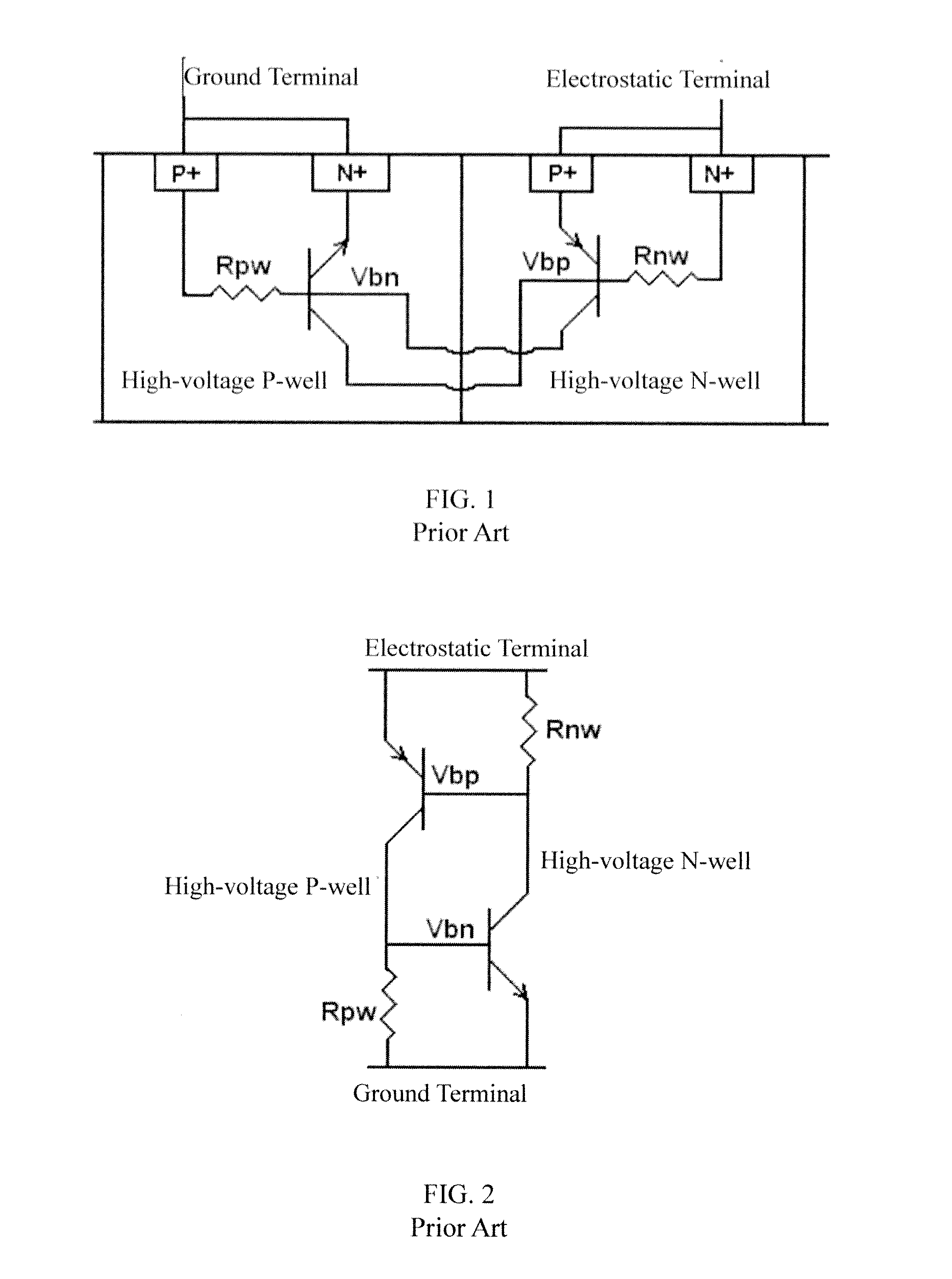
[0058]the silicon controlled rectifier comprises a high-voltage P-well and a high-voltage N-well; the high-voltage P-well and the high-voltage N-well are adjacent to each other;

[0059]a first N+ diffusion region and a first P+ diffusion region are formed in the high-voltage P-well;

[0060]a sec...

embodiment 4

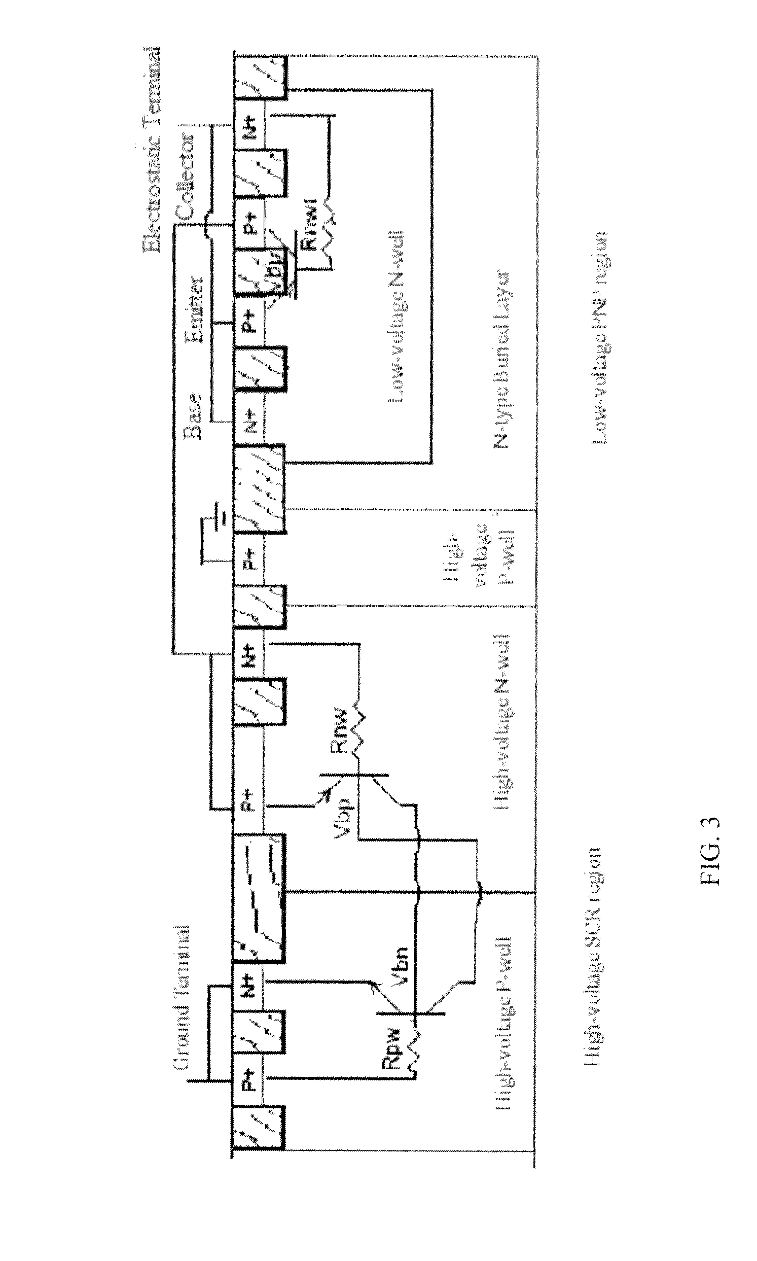
[0068]FIG. 6 shows the cross-sectional structure of a high-voltage ESD protection device in Embodiment 4 of the present invention. As shown in FIG. 6, the high-voltage ESD protection device comprises a silicon controlled rectifier and a first PMOS transistor, wherein:

[0069]the silicon controlled rectifier and the first PMOS transistor are formed on a P-type epitaxial layer of a silicon substrate;

[0070]an isolation high-voltage P-well is formed on the P-type epitaxial layer of the silicon substrate between the silicon controlled rectifier and the first PMOS transistor and the isolation high-voltage P-well isolates the silicon controlled rectifier from the first PMOS transistor;

[0071]the silicon controlled rectifier comprises a high-voltage P-well and a high-voltage N-well; the high-voltage P-well and the high-voltage N-well are adjacent to each other;

[0072]a first N+ diffusion region and a first P+ diffusion region are formed in the high-voltage P-well;

[0073]a second N+ diffusion reg...


PUM


Abstract

The present invention discloses a high-voltage ESD protection device including a silicon controlled rectifier and a first PNP transistor. The silicon controlled rectifier includes a high-voltage P-well and N-well; a first N+ and P+ diffusion region are formed in the high-voltage P-well; a second N+ and P+ diffusion region are formed in the high-voltage N-well. The first PNP transistor comprises an N-type buried layer; a low-voltage N-well formed in the N-type buried layer; and a base, emitter and collector formed in the low-voltage N-well. The base and emitter are shorted together; the collector is shorted to the second N+ diffusion region and the second P+ diffusion region; the first N+ diffusion region is shorted to the first P+ diffusion region to act as a ground terminal. The high-voltage ESD protection device can effectively adjust the ESD trigger voltage and improve the snapback sustaining voltage after the device is switched on.

Description

CROSS-REFERENCES TO RELATED APPLICATIONS[0001]This application claims the priority of Chinese patent application number 201010511125.2, tiled on Oct. 19, 2010, the entire contents of which are incorporated herein by reference.TECHNICAL FIELD[0002]The present invention relates to an ESD protection technology for semiconductor devices, especially to a high-voltage ESD protection device.BACKGROUND OF THE INVENTION[0003]As an ESD protection device, a silicon controlled rectifier (SCR) has an electrostatic discharge ability higher than, generally 5˜7 times higher than, that of a metal oxide semiconductor field effect transistor (MOSFET). FIG. 1 shows a schematic diagram of the cross-sectional structure of an existing high trigger voltage silicon controlled rectifier, wherein a collector of a parasitic PNP transistor composed of P+ region / high-voltage N-well / high-voltage P-well acts as a base of a parasitic NPN transistor composed of N+ region / high-voltage P-well / high-voltage N-well; simi...

Claims


Application Information

Patent Timeline
IPC IPC(8): H01L27/06
CPCH01L27/0262H02H9/046H01L29/7436H01L29/735
Inventor SU, QING
Owner SHANGHAI HUAHONG GRACE SEMICON MFG CORP
Why Eureka
Try Eureka