Structure and method for simultaneously forming a through silicon via and a deep trench structure

Active Publication Date: 2012-04-19
GLOBALFOUNDRIES US INC
View PDF10 Cites 67 Cited by
  • Summary
  • Abstract
  • Description
  • Claims
  • Application Information

AI Technical Summary

Problems solved by technology

Deep trench etching is very challenging and costly.
Given the high-aspect ratio of deep trenches, however, processing one type of trench (e.g.

Method used


Image

  • Structure and method for simultaneously forming a through silicon via and a deep trench structure
  • Structure and method for simultaneously forming a through silicon via and a deep trench structure
  • Structure and method for simultaneously forming a through silicon via and a deep trench structure

Examples


Embodiment Construction

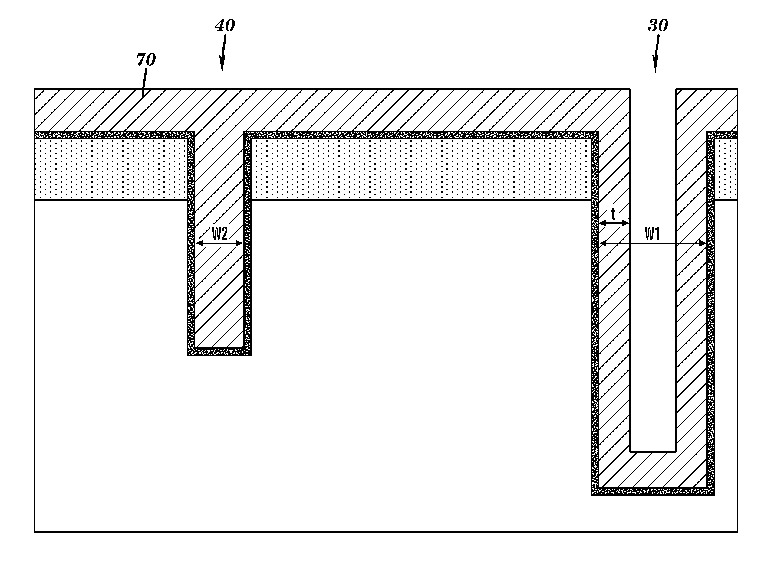
[0016]Disclosed herein is a structure and method for simultaneously forming a TSV and a DTCap or DTI on the same chip. By taking advantage of reactive ion etching (RIE) loading effects in deep trenches, a narrow DTCap or DTI trench and a wide TSV trench can be formed by a single mask and a single trench RIE, resulting in the TSV trench being deeper than the DTCap or DTI trench. A TSV and DTCap or DTI are formed with different dielectric materials on the trench sidewalls, improving device performance, without requiring any extra mask and lithography. The TSV and DTCap or DTI are perfectly aligned. No misalignment occurs.

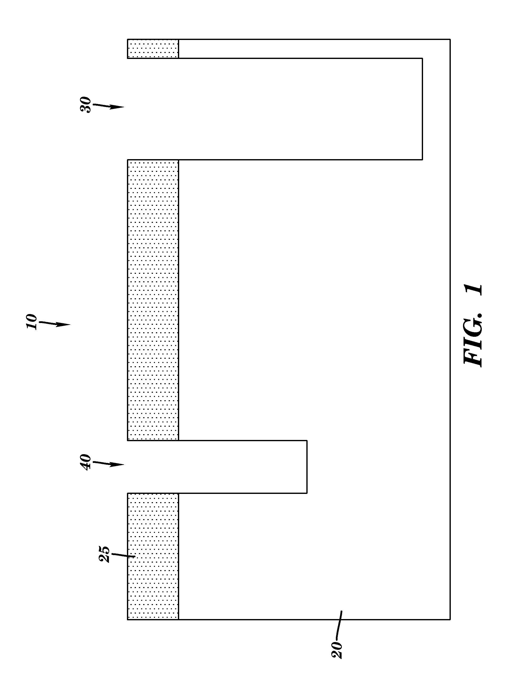
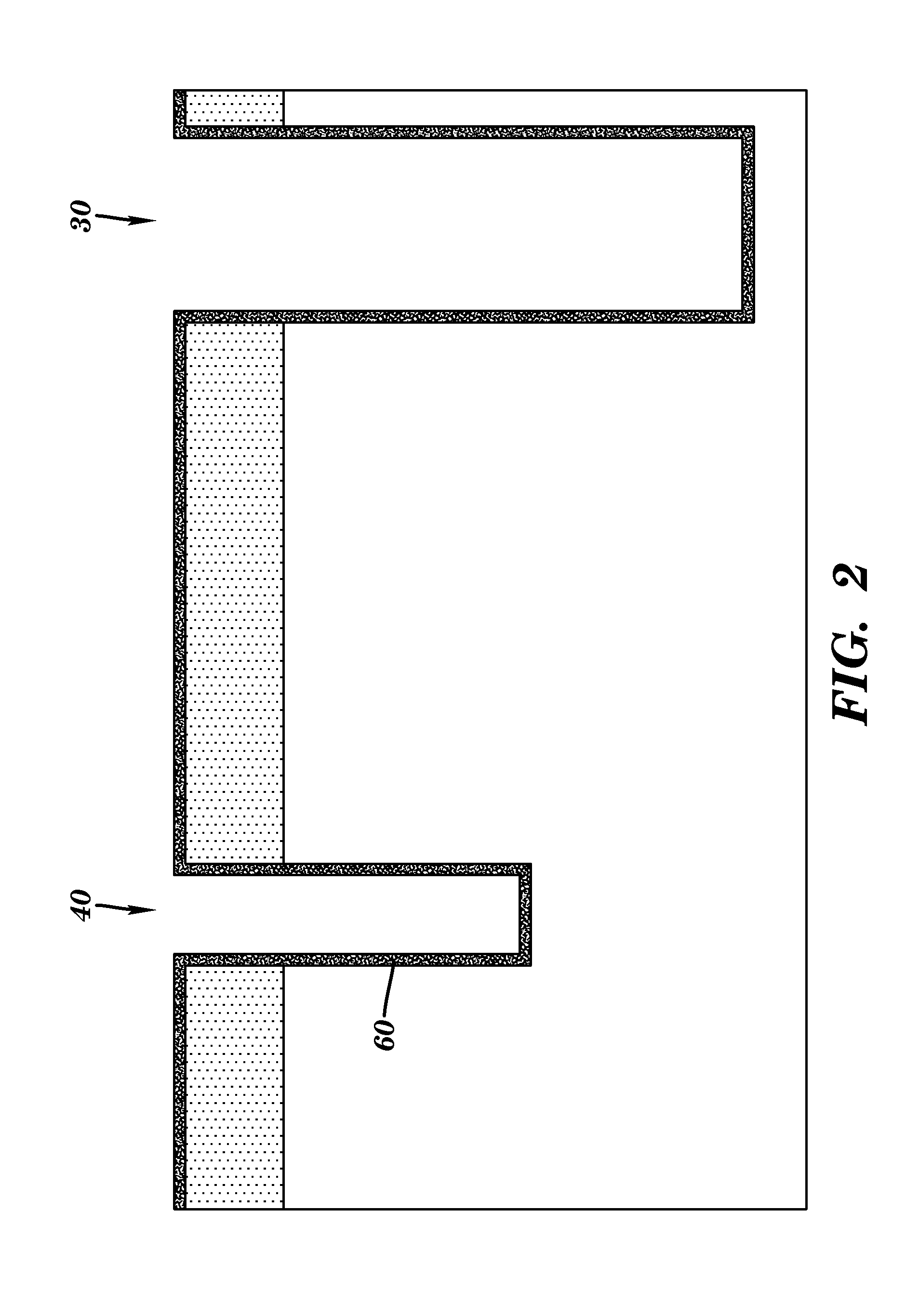
[0017]Referring to FIG. 1, a starting structure 10 includes a substrate 20. Substrate 20 may be a bulk semiconductor substrate, such as silicon, germanium or silicon germanium, a semiconductor-on-insulator (SOI) or other substrate known in the art. A pad film 25 is deposited on top of substrate 20. Pad film 25 may be deposited by conventional deposition methods such a...


PUM


Abstract

A through silicon via (TSV) and a deep trench capacitor (DTCap) or a deep trench isolation (DTI) are simultaneously formed on the same substrate by a single mask and a single reactive ion etching (RIE). The TSV trench is wider and deeper that the DTCap or DTI trench. The TSV and DTCap or DTI are formed with different dielectric materials on the trench sidewalls. The TSV and DTCap or DTI are perfectly aligned.

Description

BACKGROUND OF THE INVENTION[0001]The present invention relates generally to a method for simultaneously forming a through silicon via and a deep trench structure and, more specifically, to structures and methods for simultaneously forming a through silicon via and a deep trench capacitor or a deep trench isolation.[0002]Through-silicon-via (TSV) is becoming a viable technology approach for improving chip performance at the system level by 3-D chip integration. On-chip decoupling capacitors are highly desired to suppress power fluctuation. Deep trench capacitors (DTCap) have a capacitance density advantage over other planar capacitors due to the fact that the capacitors can be formed in deep trenches in a semiconductor substrate. Furthermore, deep trench isolation (DTI) is becoming necessary for future CMOS technologies and beyond. Deep trench etching is very challenging and costly. The issue is exacerbated due to different and sometimes competing requirements of TSV, DTCap, and DTI....

Claims


Application Information

Patent Timeline
IPC IPC(8): H01L23/538G06F17/50H01L21/768
CPCH01L21/743H01L27/0207G06F17/5081H01L21/76898H01L21/763G06F30/398
Inventor CHENG, KANGGUOFAROOQ, MUKTA G.HSU, LOUIS L.
Owner GLOBALFOUNDRIES US INC
Why Eureka
Try Eureka