Color conversion film using polymeric dye, and multicolor light-emitting organic el device using same
- Summary
- Abstract
- Description
- Claims
- Application Information
AI Technical Summary
Benefits of technology
Problems solved by technology
Method used
Image
Examples
example 1
[0072]In the following example, the formation of a color conversion film is described.
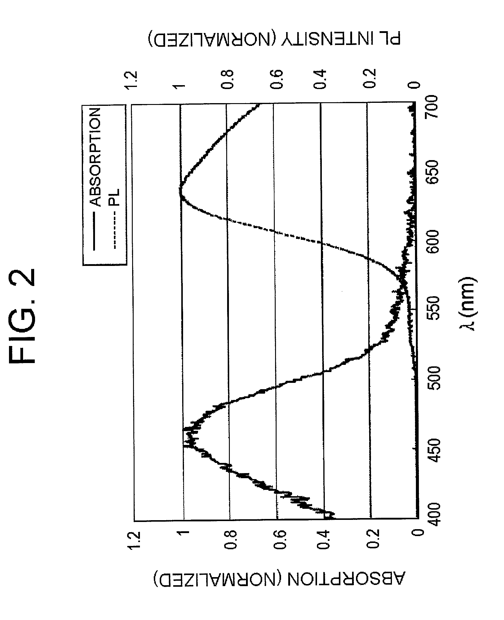
[0073]Corning 1737 glass with dimensions of 50×50×0.7 mm that had been rinsed with pure water and dried was used as the transparent glass substrate. Using fluorene / (2-methoxy-5-(2-ethylhexyloxy)-1,4-phenylene)vinylene recurring units exemplified by the formula (a) as the first dye units and a perylene compound as the second dye units, a polymeric dye material (weight-average molecular weight, 15,000) having a morphology wherein the second dye units have been introduced onto a main chain of the first dye units was prepared. This polymeric dye material was dissolved in a mesitylene solvent to a concentration of 1 wt %. The glass substrate was set on a spin coater, and the substrate was spun while dripping the polymeric dye solution thereon, thereby forming a uniform film. In the spin coating operation, the substrate was spun for 3 minutes at a spin rate of 800 rpm. The color conversion film of this e...
example 2
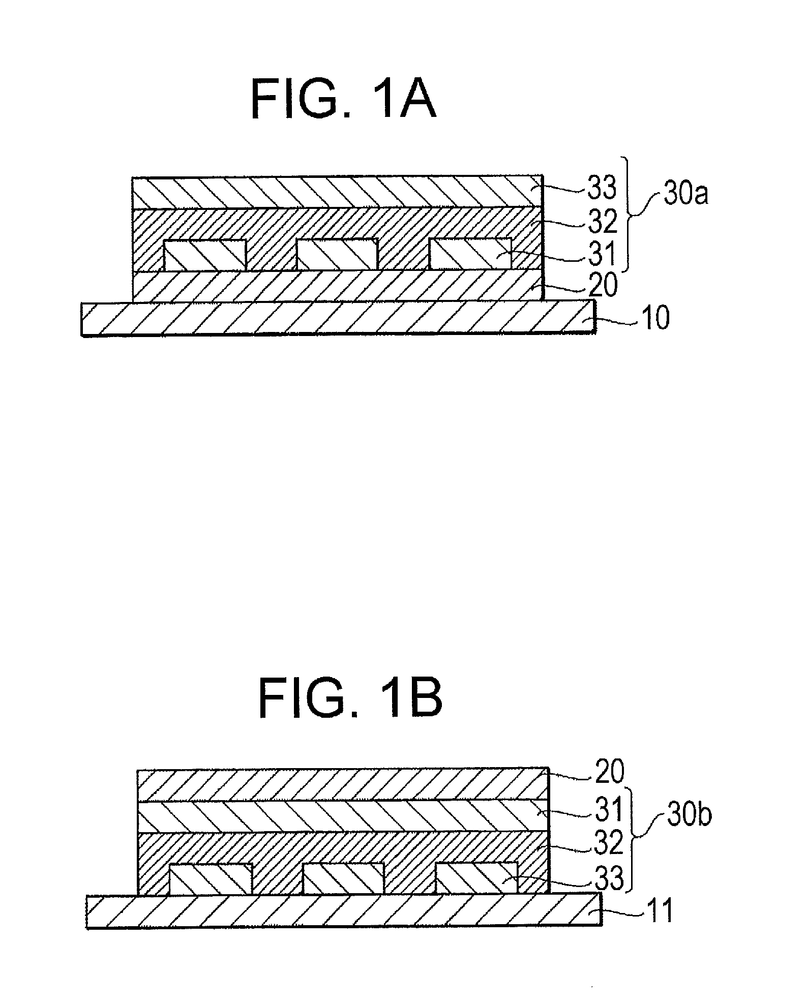
[0080]This is an example in which the top emission-type device shown in FIG. 1B was fabricated.
[0081]Corning 1737 glass with dimensions of 50×50×0.7 mm that had been rinsed with pure water and dried was used as the transparent glass substrate. The transparent glass substrate was carried into a sputtering system, where a CrB film having a thickness of 200 nm was formed using a DC magnetron sputtering process. Following film formation, the substrate was removed from the sputtering system and four stripe-shaped electrodes having linewidths of 2 mm and 2 mm intervals therebetween were formed by a photolithographic process, thereby creating a reflecting electrode. The commercially available photoresist AZ-1500 (AZ Electronics Materials KK) and the commercially available etchant Cr-01 N (Kanto Chemical Co., Inc.) were used in photolithographic patterning.
[0082]The substrate on which the reflecting electrode had been formed was carried into a vacuum deposition system. First, a mask having ...
PUM
| Property | Measurement | Unit |
|---|---|---|
| Fraction | aaaaa | aaaaa |
| Fraction | aaaaa | aaaaa |
| Thickness | aaaaa | aaaaa |
Abstract
Description
Claims
Application Information


