Color conversion film using polymeric dye, and multicolor light-emitting organic EL device using same
a technology of polymeric dye and conversion film, which is applied in the direction of discharge tube luminescnet screen, organic semiconductor device, discharge tube/lamp details, etc., can solve the problem of not obtaining sufficient conversion light intensity, reducing the concentration of color conversion material, and reducing the absorbance of light to be absorbed, so as to achieve low viewing angle dependence, high color conversion efficiency, and the effect of reducing the aggregation of second dye units
- Summary
- Abstract
- Description
- Claims
- Application Information
AI Technical Summary
Benefits of technology
Problems solved by technology
Method used
Image
Examples
example 1
[0074]In the following example, the formation of a color conversion film is described.
[0075]Corning 1737 glass with dimensions of 50×50×0.7 mm that had been rinsed with pure water and dried was used as the transparent glass substrate. Using fluorene / (2-methoxy-5-(2-ethylhexyloxy)-1,4-phenylene)vinylene recurring units exemplified by the formula (a) as the first dye units and a perylene compound as the second dye units, a polymeric dye material (weight-average molecular weight, 15,000) having a morphology wherein the second dye units have been introduced onto a main chain of the first dye units was prepared. This polymeric dye material was dissolved in a mesitylene solvent to a concentration of 1 wt %. The glass substrate was set on a spin coater, and the substrate was spun while dripping the polymeric dye solution thereon, thereby forming a uniform film. In the spin coating operation, the substrate was spun for 3 minutes at a spin rate of 800 rpm. The color conversion film of this e...
example 2
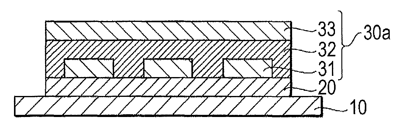
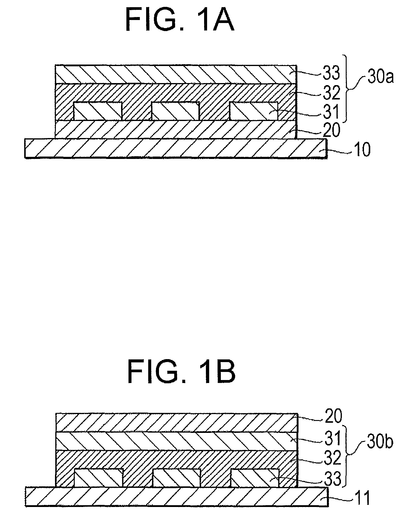
[0083]This is an example in which the top emission-type device shown in FIG. 1B was fabricated.
[0084]Corning 1737 glass with dimensions of 50×50×0.7 mm that had been rinsed with pure water and dried was used as the transparent glass substrate. The transparent glass substrate was carried into a sputtering system, where a CrB film having a thickness of 200 nm was formed using a DC magnetron sputtering process. Following film formation, the substrate was removed from the sputtering system and four stripe-shaped electrodes having linewidths of 2 mm and 2 mm intervals therebetween were formed by a photolithographic process, thereby creating a reflecting electrode. The commercially available photoresist AZ-1500 (AZ Electronics Materials KK) and the commercially available etchant Cr-01 N (Kanto Chemical Co., Inc.) were used in photolithographic patterning.
[0085]The substrate on which the reflecting electrode had been formed was carried into a vacuum deposition system. First, a mask having ...
PUM
| Property | Measurement | Unit |
|---|---|---|
| thickness | aaaaa | aaaaa |
| thickness | aaaaa | aaaaa |
| transmittance | aaaaa | aaaaa |
Abstract
Description
Claims
Application Information


