Multi-touch panel capacitance sensing circuit

a capacitance sensing circuit and multi-touch technology, applied in the field of multi-touch panel capacitance sensing circuits, can solve the problems of inability to directly convert the flow of charge into a voltage and then processed, the function of such electronic equipment cannot be accurately sensed, and the effect of high toleran

Inactive Publication Date: 2012-04-19
POINTCHIPS CO LTD
View PDF1 Cites 26 Cited by
  • Summary
  • Abstract
  • Description
  • Claims
  • Application Information

AI Technical Summary

Benefits of technology

[0027]Accordingly, the present invention has been made keeping in mind the above problems occurring in the prior art, the present invention improves the problems of conventionally used capacitance sensing circuits when implementing a touch panel device using a mutual cap method which supports multi-touc

Problems solved by technology

As the various types of electronic equipment are used in daily life and the functions of such electronic equipment becomes advanced and complicated, the necessity of a user interface which can be easily learned and intuitively manipulated by a user has arisen.
Therefore, there is the basic problem of two or more points of multi-touch cannot be able to be accurately sensed.
Due to the weak flow of charge, the flow of charge cannot be directly converted to a voltage and then processed.
However, such an integration circuit is disadvantageous in that an insignificant current is transferred to a reception unit side because it is very difficult to match transmission impedance with reception impedance, and in that voltage cannot be accurately maintained after integration was performed because output voltage varies due to integration draft when charge is integrated using an OPAMP.
Further, as shown in FIG. 4 which illustrates operational voltages of the respective circuits of FIG. 3, integration Vint can be performed at only the rising edge 260 or falling edge 261 of each period of the square-wave-type transmission waveform TX of FIG. 4 in response to an integration control signal 241, so that the

Method used


Image

  • Multi-touch panel capacitance sensing circuit
  • Multi-touch panel capacitance sensing circuit
  • Multi-touch panel capacitance sensing circuit

Examples


Embodiment Construction

[0050]Reference now should be made to the drawings, in which the same reference numerals are used throughout the different drawings to designate the same or similar components.

[0051]Hereinafter the embodiments of a multi-touch panel capacitance sensing circuit according to the present invention will be described in detail with reference to the attached drawings.

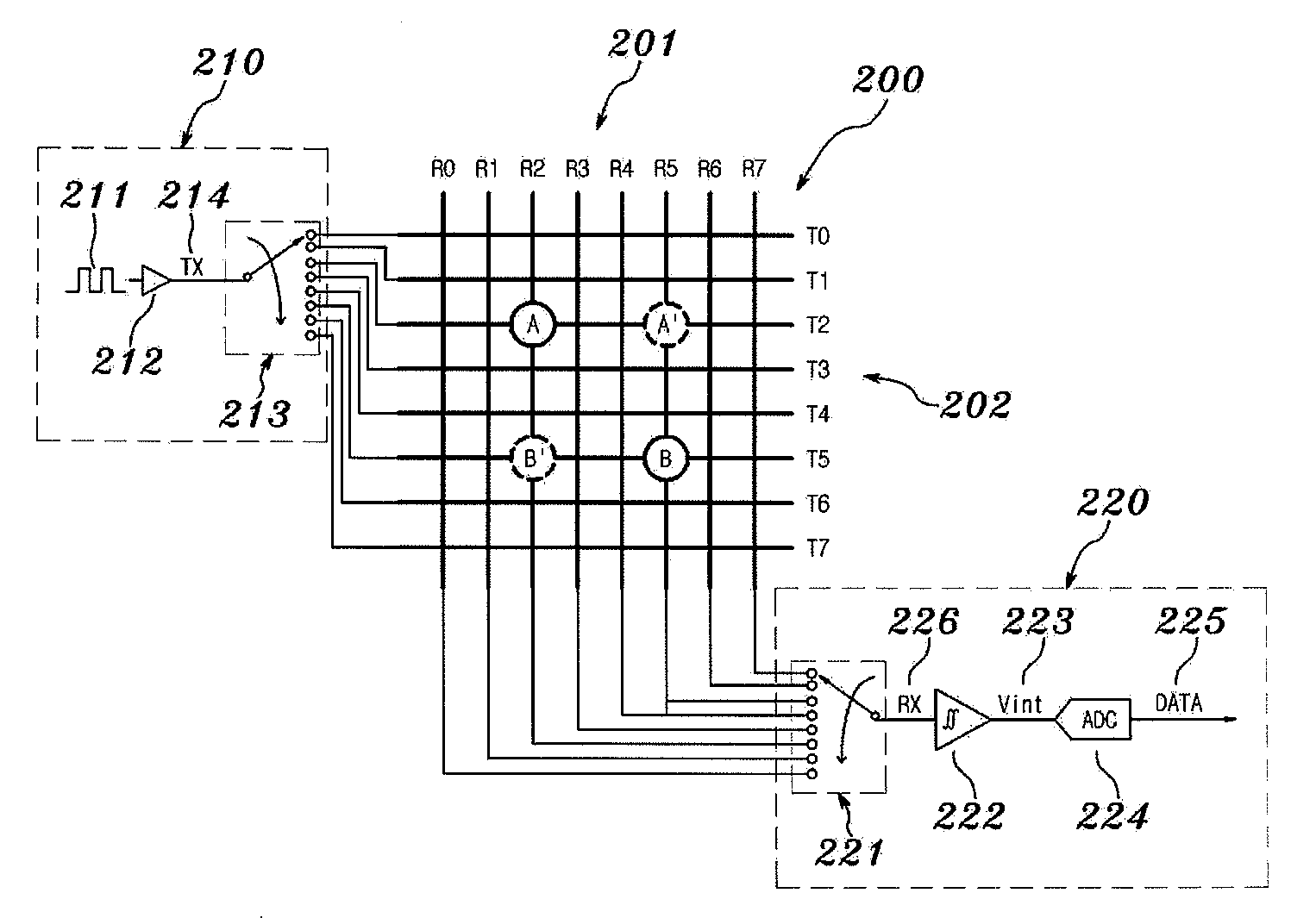
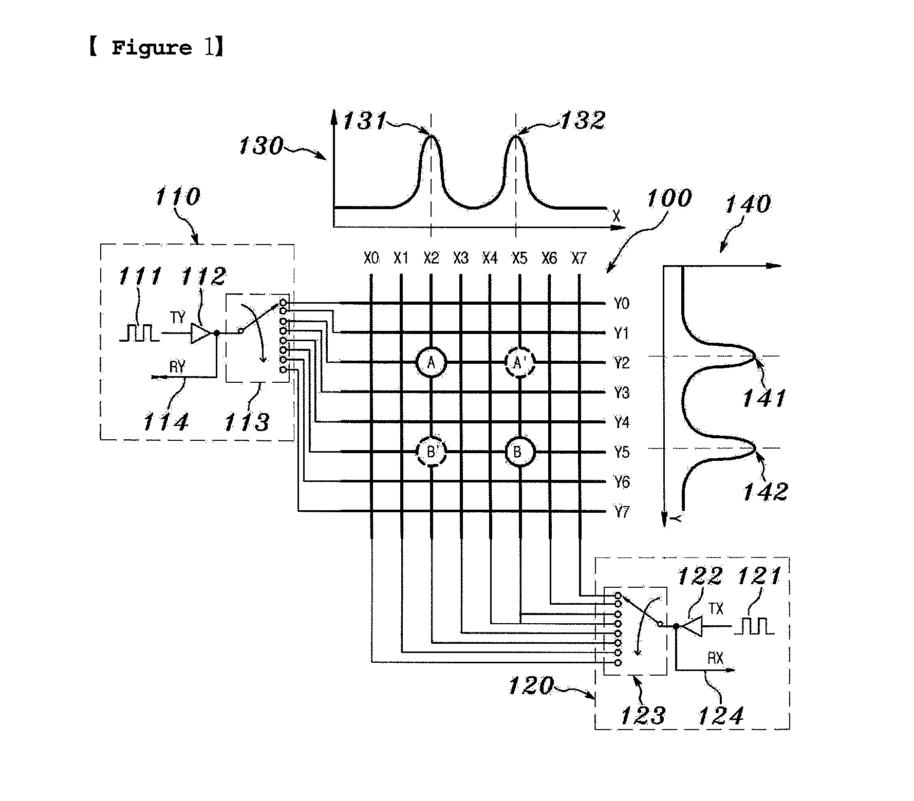
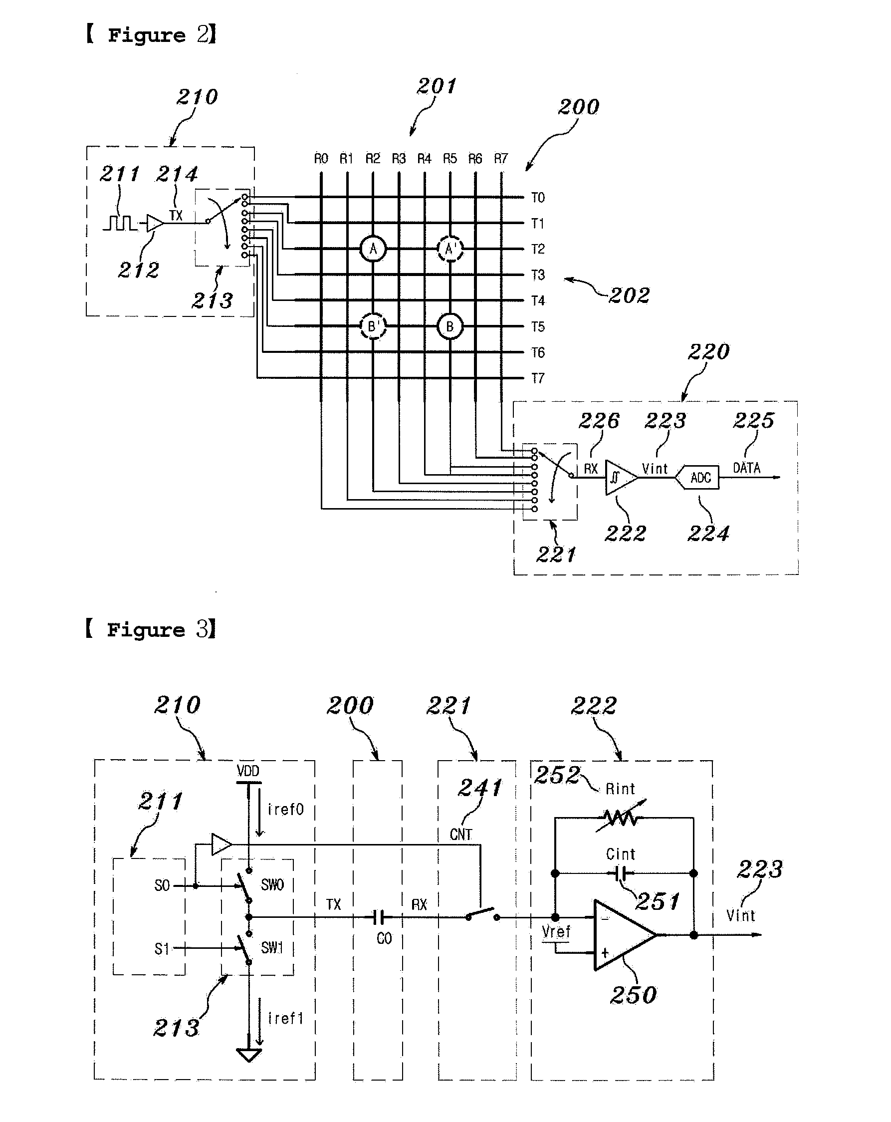
[0052]The multi-touch panel capacitance sensing circuit according to the present invention includes a touch panel having x-axis electrodes and y-axis electrodes, a transmission circuit unit 300 for applying a transmission signal, having a predetermined period, to the x-axis electrodes in a time division manner, and a reception circuit unit for detecting difference in capacitance components generated between electrodes 310, configured with an x-axis electrode and an y-axis electrode, based on the y-axis electrode. The reception circuit unit includes a current mirror-based charge integration circuit, and detects whether a touch...


PUM


Abstract

Disclosed herein is a multi-touch panel capacitance sensing circuit. The multi-touch panel capacitance sensing circuit includes a touch panel, a transmission circuit unit, and a reception circuit unit. The touch panel includes transmission electrodes and reception electrodes. The transmission circuit unit applies a transmission signal, having a predetermined period, to the transmission electrodes in a time division manner. The reception circuit unit for detecting a difference in capacitance components, generated between the transmission electrode and the reception electrode, based on the reception electrode when a touch is generated by the human body of a user. The reception circuit unit includes a current mirror-based charge integration circuit, and detects whether a touch is generated or not.

Description

BACKGROUND OF THE INVENTION[0001]1. Field of the Invention[0002]The present invention relates generally to a multi-touch panel capacitance sensing circuit, and, more particularly, to a capacitance sensing circuit which is robust to noise flowing in from the outside, which has a high sensing speed, and which can be easily manufactured.[0003]2. Description of the Related Art[0004]With the development of electronics and information technology, the importance of electronic equipment, which occupies a large part of everyday life including the business environment, has constantly increased. Recently, the types of electronic equipment have become diversified. In particularly, newly designed equipment to which new functions are applied pours out every day in the field of mobile electronic equipment, such as notebooks, mobile phones, Portable Multimedia Players (PMPs), and tablet Personal Computers (PCs),[0005]As the various types of electronic equipment are used in daily life and the functi...

Claims


Application Information

Patent Timeline
IPC IPC(8): G06F3/044
CPCG06F3/044G06F3/0416G06F3/0446G06F3/04182G06F2203/04104G06F2203/04103G06F2203/04111G06F3/04164G06F3/04166
Inventor HAN, SANG HYUN
Owner POINTCHIPS CO LTD
Why Eureka
Try Eureka