
Solar cell apparatus and method of fabricating the same

a solar cell and apparatus technology, applied in the field can solve problems such as degrading electrical characteristics of solar cells, and achieve the effects of improving the efficiency of solar cell apparatus, reducing process time, and reducing non-active area naa

Inactive Publication Date: 2012-05-10
LG INNOTEK CO LTD
View PDF5 Cites 5 Cited by
  • Summary
  • Abstract
  • Description
  • Claims
  • Application Information

AI Technical Summary

Benefits of technology

[0010]According to the embodiment, the back electrode layer, the light absorption layer, and the front electrode layer are formed by performing deposition and patterning processes at the same time by means of the mask. Thus, an addition process such as laser patterning or mechanical scribing is unnecessary.
[0011]Thus, the back electrode layer, the light absorption layer, and the front electrode layer can be formed all in a vacuum, and the process time can be reduced.
[0012]In addition, when the back electrode layer, the light absorption layer, and the front electrode layer are formed, the mask is used in the patterning process, and thus, the back electrode layer, the light absorption layer, and the front electrode layer can be protected from a mechanical shock. That is, ripping of the back electrode layer, the light absorption layer, and the front electrode layer due to a process such as mechanical scribing can be prevented.
[0013]In addition, since the patterning process can be more precisely performed than a mechanical patterning process, the non-active area NAA can be decreased, thereby improving the efficiency of the solar cell apparatus.
[0014]In addition, since the inner surfaces of the light absorption layer defining the recesses are inclined, the material used to form the front electrode layer can be efficiently deposited on the inner surfaces, thereby forming contact patterns.
[0015]In addition, the inner surfaces of the light absorption layer defining the recesses may be connected to the top surface of the light absorption layer through a round portion. Thus, breakage between the contact pattern and the front electrode layer can be prevented.

Problems solved by technology

In addition, each layer may be ripped off through a mechanical patterning process, or layers adjacent to a pattern may be burred through a laser patterning process, which degrade electrical characteristics of a solar cell.

Method used


Image

  • Solar cell apparatus and method of fabricating the same
  • Solar cell apparatus and method of fabricating the same
  • Solar cell apparatus and method of fabricating the same

Examples


first embodiment

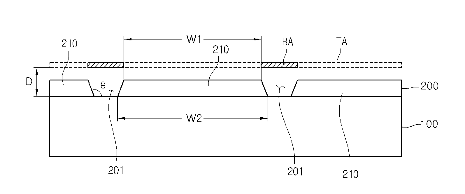
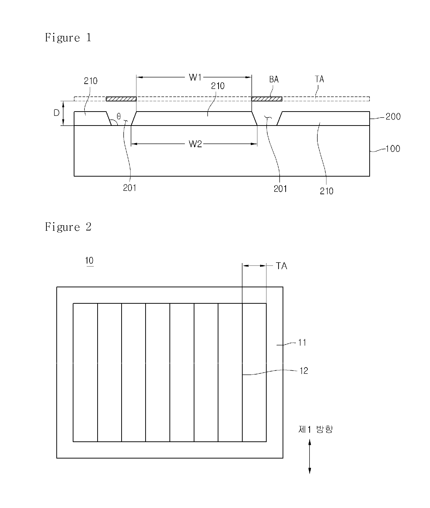
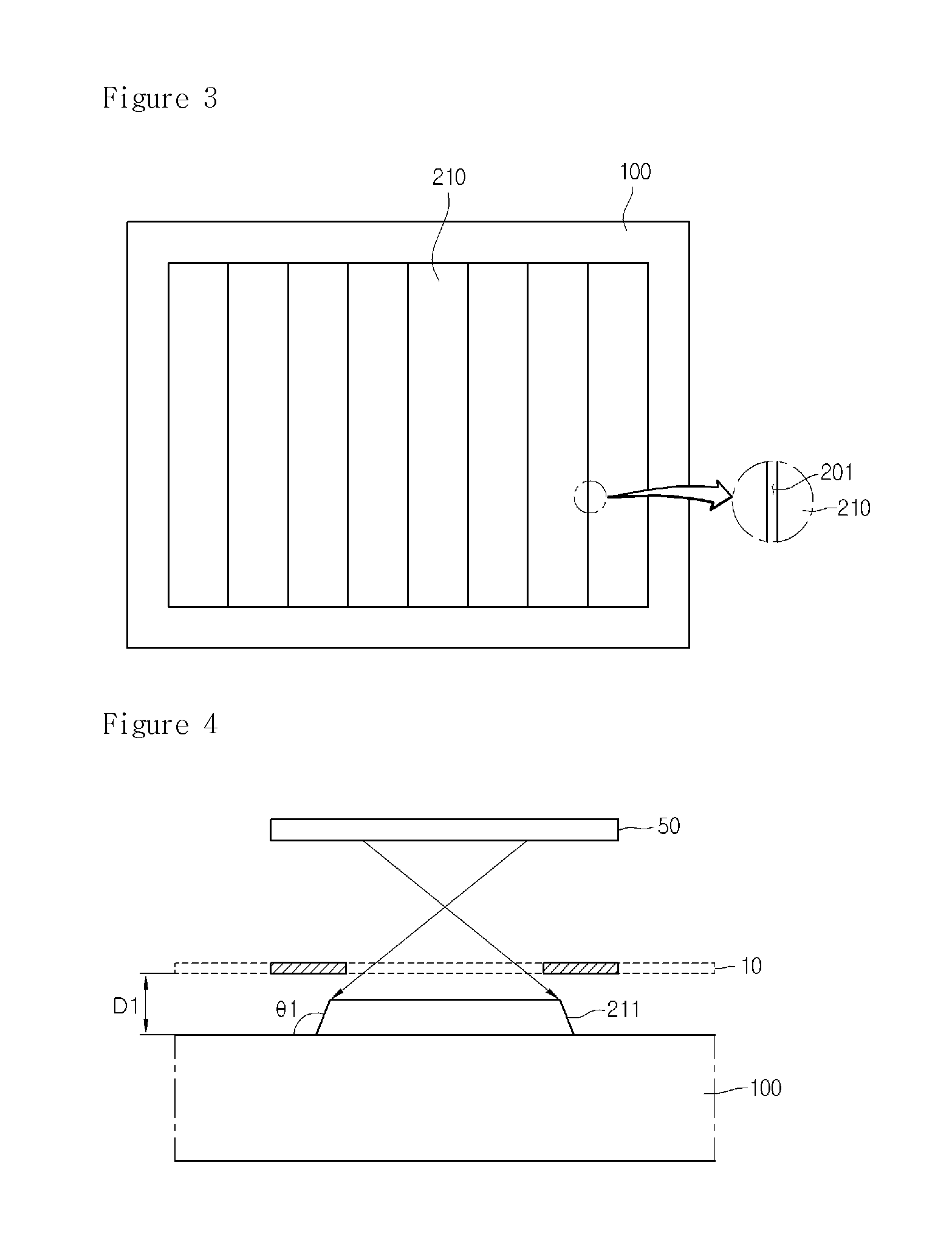
[0023]FIGS. 1 and 4 to 9 are cross-sectional views illustrating a method of fabricating a solar cell apparatus according to a FIG. 2 is a plan view illustrating a mask for forming a back electrode layer. FIG. 3 is a plan view illustrating a back electrode layer formed using the mask of FIG. 2.

[0024]Referring to FIGS. 1 and 3, a substrate 100 is prepared, and a back electrode layer 200 is formed on the substrate 100.

[0025]The substrate 100 is formed of glass, or may be formed of ceramic such as alumina, stainless steel, titanium, or polymer. Glass used to form the substrate 100 may be sodalime glass, and polymer used to form the substrate 100 may be polyimide. The substrate 100 may be rigid or flexible.

[0026]A mask 10 is placed on the substrate 100 to form the back electrode layer 200.

[0027]The mask 10 is used to selectively deposit a material on the substrate 100, thereby forming the back electrode layer 200. Referring to FIG. 2, the mask 10 may include a tetragonal frame 11 and a ...

second embodiment

[0087]FIGS. 10 to 12, and 14 to 16 are cross-sectional views illustrating a method of fabricating a solar cell according to a The current embodiment may refer to the previous embodiment. That is, the previous embodiment may be substantially coupled to the current embodiment except for modified parts.

[0088]First, referring to FIG. 10, a preliminary back electrode layer 202 is formed on the substrate 100.

[0089]A substrate 100 is formed of glass, or may be formed of ceramic such as alumina, stainless steel, titanium, or polymer. Glass used to form the substrate 100 may be sodalime glass, and polymer used to form the substrate 100 may be polyimide. The substrate 100 may be rigid or flexible.

[0090]The preliminary back electrode layer 202 is formed of a conductor such as a metal. For example, the preliminary back electrode layer 202 may be formed through a sputtering process using a molybdenum (Mo) target. Mo has high electrical conductivity, an ohmic contact with a light absorption laye...


PUM


Abstract

A solar cell apparatus and a method of fabricating the same are provided. The solar cell apparatus includes a substrate, a back electrode layer, a light absorption layer, and a front electrode layer. The back electrode layer is on the substrate. The light absorption layer is on the back electrode layer. The front electrode layer is on the light absorption layer. The back electrode layer is provided with recesses. Inner surfaces of the back electrode layer defining the recesses are inclined from a top surface of the substrate.

Description

TECHNICAL FIELD[0001]Embodiments relate to a solar cell apparatus and a method of fabricating the solar cell apparatus.BACKGROUND ART[0002]Recent increasing consumption of energy has facilitated development of solar cells capable of converting solar energy into electric energy.[0003]Particularly, CuInGaSe (CIGS) solar cells are common, which are pn hetero junction devices having a substrate structure constituted by a glass substrate, a metal back electrode layer, a p-type CIGS light absorption layer, a high resistance buffer layer, and an n-type window layer.[0004]In this case, the light absorption layer is patterned to connect electrodes to one another, and the buffer layer and the light absorption layer are patterned to form unit cells.[0005]To this end, a vacuum state should be changed to an atmospheric state. In addition, each layer may be ripped off through a mechanical patterning process, or layers adjacent to a pattern may be burred through a laser patterning process, which d...

Claims


Application Information

Patent Timeline
Patent Type & Authority Applications(United States)
IPC IPC(8): H01L31/0224H01L31/18
CPCH01L31/022425H01L31/0749H01L31/0463Y02E10/541H01L31/18Y02P70/50
Inventor CHO, HO GUN
Owner LG INNOTEK CO LTD
Learn More