Nanostructures Having Crystalline and Amorphous Phases

a technology of nanostructures and crystalline phases, applied in the field of material science, can solve the problems of only limited success in tiosub>2 /sub>application, and the real potential of tiosub>2 /sub>has not been realized

Inactive Publication Date: 2012-05-17
RGT UNIV OF CALIFORNIA
View PDF8 Cites 21 Cited by
  • Summary
  • Abstract
  • Description
  • Claims
  • Application Information

AI Technical Summary

Problems solved by technology

As a consequence, TiO2 can absorb but a small fraction of solar radiation, leaving over 90% of the energy in the solar spectrum essentially wasted.
While impurity doping is a well-established method of tuning the band gap, its application to TiO2 has had only limited success.
Nevertheless, despite decades of extensive research, the true potential of TiO2 has not been realized, as the material absorbs only in the UV portion of the solar spectrum.
Nitrogen-doped TiO2 so far exhibits the best response to solar radiation, but its absorption in the visible and infrared wavelength portions of the solar spectrum remains inefficient.

Method used


Image

  • Nanostructures Having Crystalline and Amorphous Phases
  • Nanostructures Having Crystalline and Amorphous Phases
  • Nanostructures Having Crystalline and Amorphous Phases

Examples


Embodiment Construction

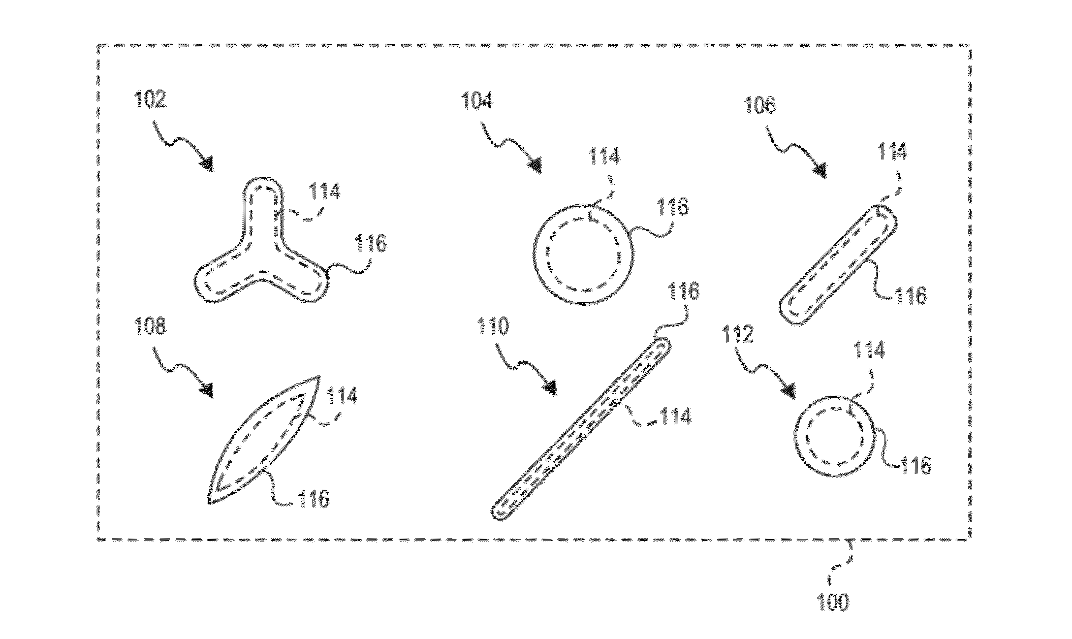
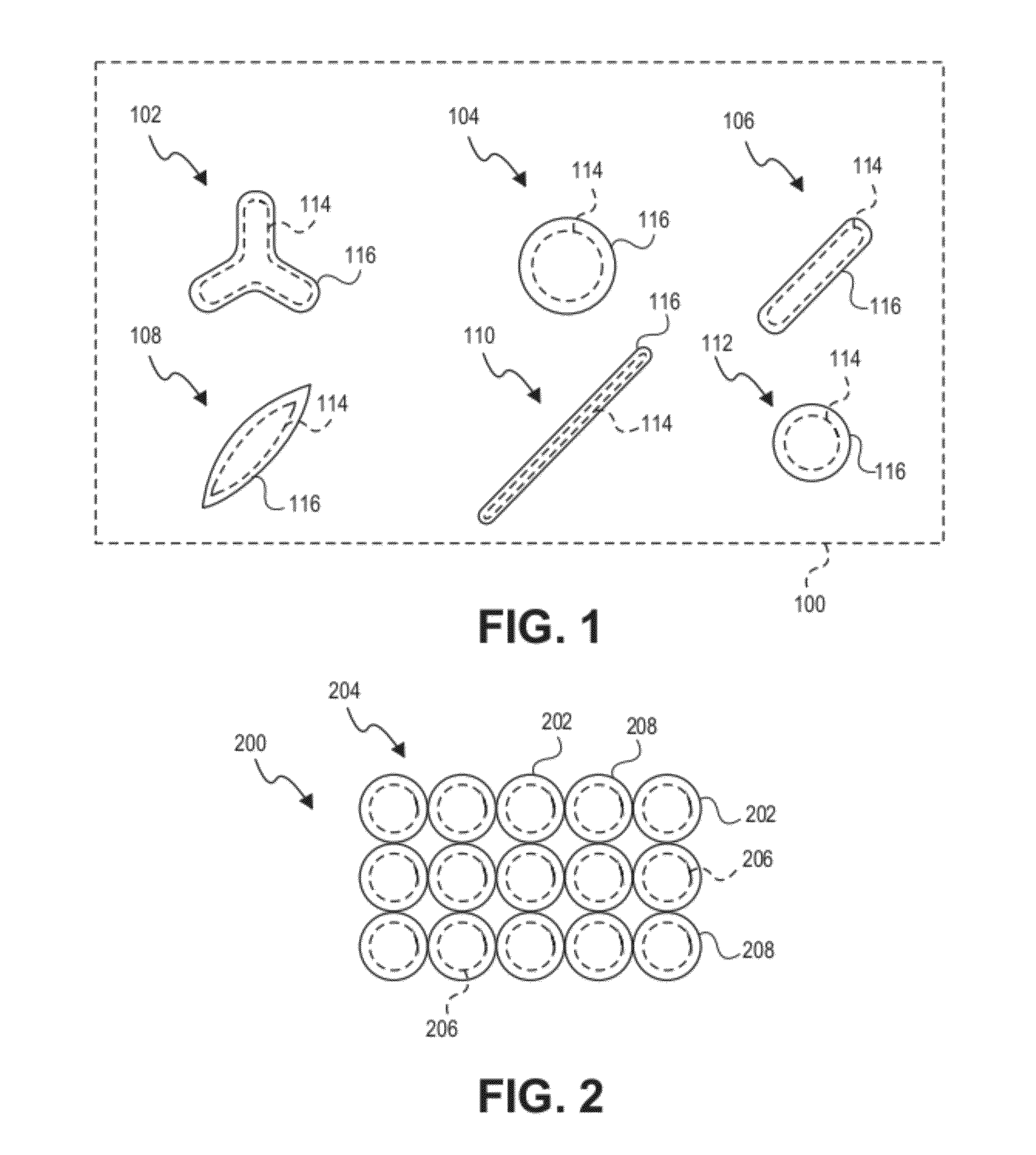
[0032]Embodiments of the present invention include a nanostructure and a method of making the nanostructure. The nanostructure may be a nanoparticle or a collection of nanoparticles.

[0033]An embodiment of a nanostructure of the present invention includes a crystalline phase and an amorphous phase. The amorphous phase is in contact with the crystalline phase. Each of the crystalline and amorphous phases has at least one dimension on a nanometer scale. As used herein, a nanometer scale according to some embodiments is within a range of about 0.5 to 200 nm, according to other embodiments is within a range of about 0.5 to 100 nm, and according to yet other embodiments is within a range of about 0.5 nm to 1 μm. The at least one dimension for each of the crystalline and amorphous phases may be a length, a diameter, or a thickness. For example, if the nanostructure is a nanoparticle having a crystalline core and an amorphous shell, the at least one dimension for the crystalline core is a d...


PUM

PropertyMeasurementUnit
absorption edgeaaaaaaaaaa

Abstract

The present invention includes a nanostructure, a method of making thereof, and a method of photocatalysis. In one embodiment, the nanostructure includes a crystalline phase and an amorphous phase in contact with the crystalline phase. Each of the crystalline and amorphous phases has at least one dimension on a nanometer scale. In another embodiment, the nanostructure includes a nanoparticle comprising a crystalline phase and an amorphous phase. The amorphous phase is in a selected amount. In another embodiment, the nanostructure includes crystalline titanium dioxide and amorphous titanium dioxide in contact with the crystalline titanium dioxide. Each of the crystalline and amorphous titanium dioxide has at least one dimension on a nanometer scale.

Description

RELATED APPLICATIONS[0001]This application claims priority to PCT Application PCT / US2010 / 026081 filed Mar. 3, 2010, which in turn claims priority to U.S. Provisional Patent Application Ser. Nos. 61 / 159,759, filed Mar. 12, 2009; 61 / 163,856, filed Mar. 26, 2009; and, 61 / 180,208, filed May 21, 2009; which are hereby incorporated by reference in their entireties.STATEMENT OF GOVERNMENT SUPPORT[0002]This invention was made with government support under Contract No. DE-AC02-05CH11231 awarded by the U.S. Department of Energy. The government has certain rights in this invention.BACKGROUND OF THE INVENTION[0003]The present invention relates to the field of material science and, more particularly, to the field of material science which includes nanostructures. The present invention also relates to the field of chemistry and, more particularly, to the field of photocatalysis.[0004]Material science has uncovered semiconductors with electronic properties that are strikingly beneficial to a numbe...

Claims


Application Information

Patent Timeline
Patent Type & Authority Applications(United States)
IPC IPC(8): C01B3/04B01J21/06B01J37/00B01J37/02B01J19/12B01J35/02B01J37/34B82Y30/00
CPCB01J21/063C02F1/725B01J35/0006B01J35/002B01J35/004B01J37/349B82Y30/00C01G23/047C01P2002/72C01P2002/85C01P2004/04C01P2004/64C01P2006/40C02F1/32B01J23/42B01J19/127B01J37/033B01J37/10B01J2219/1203Y02E60/36Y10S977/762B01J35/02B01J37/0072B01J37/0215B01J37/0221B01J37/347C01B3/042
Inventor MAO, SAMUEL S.CHEN, XIAOBO
Owner RGT UNIV OF CALIFORNIA
Why Eureka
Try Eureka