ESD protection device and manufacturing method thereof
a protection device and manufacturing method technology, applied in the direction of resistor details, emergency protection arrangements for limiting excess voltage/current, coatings, etc., can solve the problems of difficult path creation, component limitation, critical pvc, etc., to achieve high reliability, reduce the starting voltage or the peak voltage, and achieve the effect of high reliability
- Summary
- Abstract
- Description
- Claims
- Application Information
AI Technical Summary
Benefits of technology
Problems solved by technology
Method used
Image

Examples
example 1
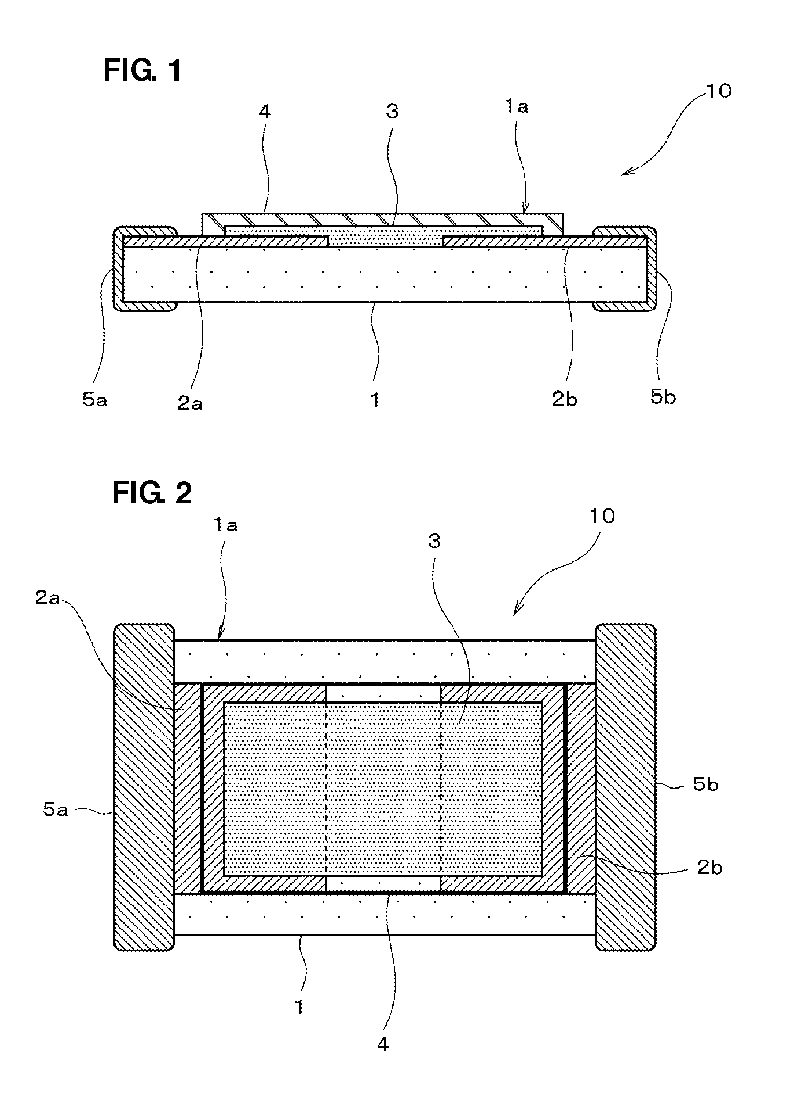
[0048]FIG. 1 is a front cross-sectional view schematically illustrating the structure of an ESD protection device according to an example (Example 1) of a preferred embodiment of the present invention, and FIG. 2 is a plan view thereof.
[0049]This ESD protection device 10 preferably includes, as shown in FIGS. 1 and 2, a ceramic base material 1, a pair of opposed electrodes 2a and 2b located on the ceramic base material 1, a discharge auxiliary electrode film 3 located between the pair of opposed electrodes 2a and 2b, a protective film 4 provided on the discharge auxiliary electrode film 3, and terminal electrodes 5a and 5b providing external electrical connections, which are provided on both ends of the ceramic base material 1 so as to provide conduction to the opposed electrodes 2a and 2b.
[0050]In Example 1, an alumina substrate which has a rectangular planar shape of about 1.0 mm in length, about 0.5 mm in width, and about 0.3 mm in thickness, for example, is preferably used as t...
modification example
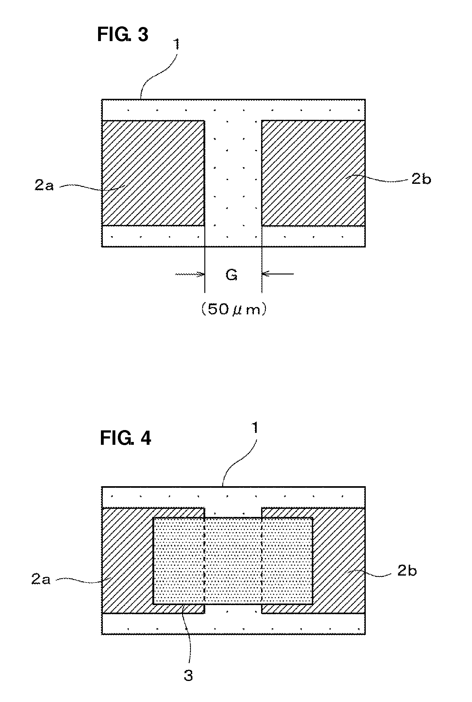
[0116]FIG. 8 illustrates a modification example of the ESD protection device according to Example 1. This ESD protection device in FIG. 8 preferably has a structure in which a barrier layer 21 containing inorganic insulating material particles (alumina particles in Example 1) as its main constituent is arranged so as to lie between the discharge auxiliary electrode film 3 and the tip sections of the pair of opposed electrodes 2a and 2b and the ceramic base material 1.
[0117]In this ESD protection device in FIG. 8, some of the glass (the glass covering the metallic particles) included in the discharge auxiliary electrode film 3 penetrates through the barrier layer 21 to prevent and suppress local excessive sintering between the metallic particles constituting the discharge auxiliary electrode film 3, thus allowing variation in initial insulation resistance to be reduced, and allowing an ESD protection device to be provided which has stable characteristics.
example 2
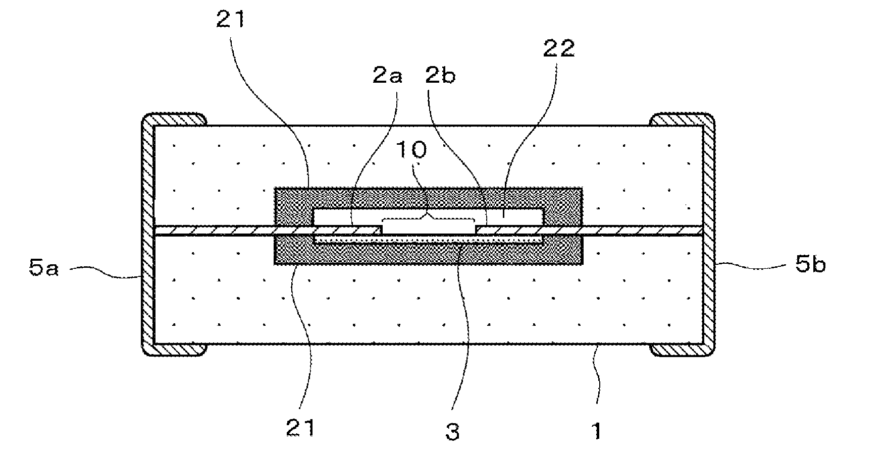
[0118]FIG. 9 is a front cross-sectional view schematically illustrating the structure of an ESD protection device according to another example (Example 2) of a preferred embodiment of the present invention.
[0119]This ESD protection device 10 includes, as shown in FIG. 9, a pair of opposed electrodes 2a and 2b with tip sections provided in a cavity section 22 in a ceramic base material 1, a discharge auxiliary electrode film 3 provided between the pair of opposed electrodes 2a and 2b, and terminal electrodes 5a and 5b for external electrical connections, which are provided on both ends of the ceramic base material 1 so as to provide conduction to the opposed electrodes 2a and 2b.
[0120]Furthermore, in this ESD protection device according to Example 2, a barrier layer 21 containing insulating material particles (alumina particles in this example) as its main constituent is arranged so as to surround a section to serve as the ESD protection device, that is, a cavity section 22 provided...
PUM
| Property | Measurement | Unit |
|---|---|---|
| softening point | aaaaa | aaaaa |
| temperature | aaaaa | aaaaa |
| temperature | aaaaa | aaaaa |
Abstract
Description
Claims
Application Information
 - R&D
- Intellectual Property
- Life Sciences
- Materials
- Tech Scout
- Unparalleled Data Quality
- Higher Quality Content
- 60% Fewer Hallucinations
Browse by: Latest US Patents, China's latest patents, Technical Efficacy Thesaurus, Application Domain, Technology Topic, Popular Technical Reports.
© 2025 PatSnap. All rights reserved.Legal|Privacy policy|Modern Slavery Act Transparency Statement|Sitemap|About US| Contact US: help@patsnap.com