Optical semiconductor device and method of manufacture thereof

An optical semiconductor and device technology, which is applied in the fields of semiconductor lasers, optical head manufacturing, and laser parts, etc., can solve the problems of increasing the area of ​​the light-receiving element substrate 103, increasing the working current, and reducing the light output.

Inactive Publication Date: 2006-12-27
PANASONIC CORP
View PDF1 Cites 2 Cited by
  • Summary
  • Abstract
  • Description
  • Claims
  • Application Information

AI Technical Summary

Problems solved by technology

[0009] (1) Problem 1: Since the semiconductor laser element 101 is installed in the recess 105 on the light receiving element substrate 103, the heat generated by the light receiving element substrate 103 directly has a bad influence on the characteristics of the semiconductor laser element 101.
Due to the influence of this Joule heat, the chip temperature of the semiconductor laser element 101 rises, causing characteristic deterioration such as a decrease in light output and an increase in operating current.
In terms of methods for suppressing the influence of heat, there are methods of increasing the volume of the concave portion 105 where the semiconductor 101 is mounted, and methods of arranging the light receiving element 104 and the IV amplifier as far as possible from the semiconductor element 105. The area of ​​the light-receiving element substrate 103 is increased, resulting in an increase in cost
[0011] (2) Problem 2: Since the semiconductor laser element 101 is not sealed and is integrated with the light-receiving element substrate 103, organic gases in the atmosphere, hydrocarbons and other substances attached to the light-receiving element substrate 103 Organic gases generated from organic matter etc. adhere to the surface of the semiconductor laser element 101 and cause characteristic degradation

Method used


Image

  • Optical semiconductor device and method of manufacture thereof
  • Optical semiconductor device and method of manufacture thereof
  • Optical semiconductor device and method of manufacture thereof

Examples


Embodiment approach 1

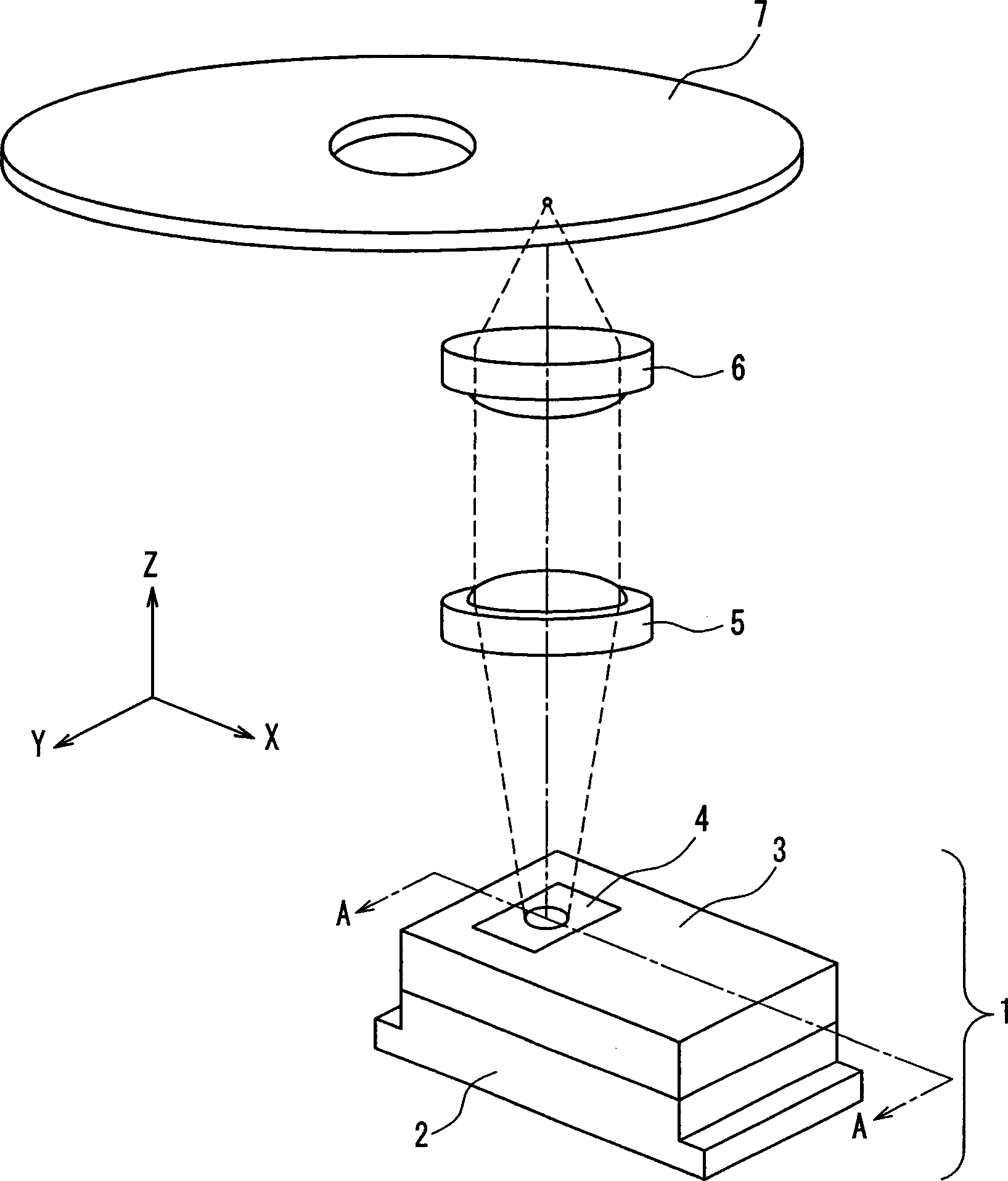
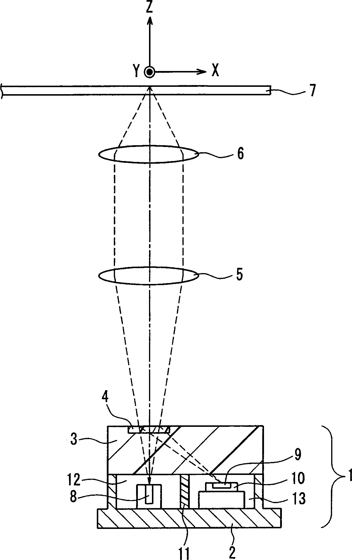
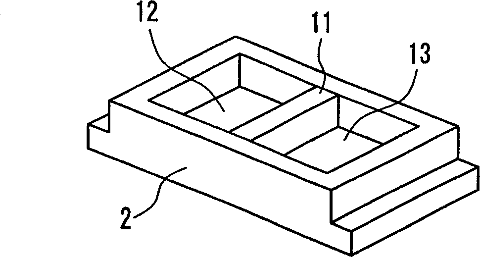
[0054] figure 1 It is a perspective view showing a disk playback device equipped with an optical semiconductor device according to Embodiment 1 as an example. Figure 2A Yes figure 1 The side view of the optical disc playback device shown, which only shows the optical semiconductor device in section ( figure 1 A-A profile in ). Figure 2B is a perspective view of the package.

[0055] exist figure 1 Among them, the optical semiconductor device 1 is constituted as an integrated structure of a package 2 and an optical module 3, wherein the package 2 has a semiconductor laser element and a light receiving element inside, and a hologram element 4 is formed in the optical module 3. The divergent light beam emitted from the semiconductor laser element is emitted from the hologram element 4 , becomes parallel light through the collimator lens 5 , and is concentrated on the information surface of the optical disc 7 through the objective lens 6 .

[0056] The light beam reflec...

Embodiment approach 2

[0070] Figure 5A It is a sectional view showing the structure of the optical semiconductor device of Embodiment 2. Figure 5B is a perspective view of the package in the device. In addition, since the configuration of the optical system other than the optical semiconductor device 1 and figure 1 are the same, so the illustration is omitted.

[0071] First, the operation of a disc playback device equipped with the optical semiconductor device of Embodiment 2 will be described.

[0072] exist Figure 5A Among them, the divergent light beam emitted from the semiconductor laser element 8 transmits the space separation element 20 and the hologram element 4 made of light-transmitting materials arranged on the exit optical axis of the semiconductor laser element, and passes through the collimator lens 5 (refer to figure 1 ) becomes parallel light, passes through the objective lens 6 (reference figure 1 ) to focus the light on disc 7 (ref. figure 1 )superior.

[0073] In ad...

Embodiment approach 3

[0089] Figure 12 It is a sectional view showing the structure of the optical semiconductor device of Embodiment 3. In addition, since the structure of the optical system other than the optical semiconductor device 1 and figure 1 are the same, so the illustration is omitted.

[0090] First, the operation of a disc playback device equipped with an optical semiconductor device will be described.

[0091] exist Figure 12 In this case, the divergent light beam emitted horizontally from the semiconductor laser element 8 is reflected by the reflective surface 15a of the first reflective element 15 inclined at 45° with respect to the outgoing optical axis, thereby changing the optical path by 90°. Afterwards, by collimating lens 5 (reference figure 1 ) becomes parallel light, which passes through the objective lens 6 (reference figure 1 ) to focus the light on disc 7 (ref. figure 1 )superior.

[0092] The reflected light beam from the optical disc 7 is incident on such as...


PUM


Abstract

Optical semiconductor device and method for manufacturing the same are provided. The optical semiconductor device includes a semiconductor laser, an optical block provided with a hologram element for diffracting a laser beam that has been emitted from the semiconductor laser and reflected by a disk, a photo-detector for receiving the laser beam diffracted by the hologram element and outputting an electric signal, and a package for receiving the semiconductor laser and the photo-detector. An internal space of the package has a plurality of independent spaces, and the semiconductor laser and the photo-detector respectively are received in the spaces that are different from each other. With this configuration, it is possible to achieve an optical semiconductor device that can be made smaller and thinner and has a highly-reliable semiconductor laser element.

Description

technical field [0001] The present invention relates to an optical semiconductor device capable of recording, reproducing, and erasing information signals on an information medium such as an optical disk, and a manufacturing method thereof. Background technique [0002] In recent years, optical discs represented by DVDs (Digital Video Discs) have been used in various fields such as audio equipment, video recorders, and computers because they can record a large amount of information at a high density. Moreover, the development and production of optical disc devices with larger capacity and higher density, such as BD (Blu-ray disc) and HD-DVD, which can record and reproduce information through blue laser light, and are considered to be further popularized in the future . Since the pickup devices incorporated in these optical disc devices are mounted on devices such as portable computers and car stereos, there are strong demands for miniaturization, thinning, and vibration res...

Claims


Application Information

Patent Timeline
Patent Type & Authority Applications(China)
IPC IPC(8): H01S5/026H01S5/022H01S5/00G11B7/125G11B7/135
CPCG11B7/1381G11B7/22G11B7/1205G11B7/1353G11B7/123G11B7/127H01S5/022Y10S430/146
Inventor 中西直树滨口真一山本博昭
Owner PANASONIC CORP
Why Eureka
Try Eureka