Power semiconductor device and preparation method thereof

A technology for power semiconductors and devices, applied in the field of power semiconductor devices, can solve the problems of complex gate drive control, unfavorable control system reliability and cost, limited reduction of reverse recovery power consumption, etc., to reduce leakage current, increase Design flexibility and design dimension, the effect of reverse recovery loss reduction

Active Publication Date: 2022-05-27
安建科技(深圳)有限公司
View PDF11 Cites 3 Cited by
  • Summary
  • Abstract
  • Description
  • Claims
  • Application Information

AI Technical Summary

Problems solved by technology

This technical solution can change the height of the Schottky barrier by changing the doping concentration of the front P-type region and the work function of the emitter metal to adjust the hole injection efficiency; however, the parameter design in this technology is limited by the RC-IGBT process, There is a limit to how much reverse recovery power can be reduced
The industry also proposes a method of controlling the gate of the IGBT cell to turn on the gate of the IGBT cell before the reverse recovery of the FWD cell, and reduce the number of carriers during reverse recovery by deriving the front electron current; but this The scheme makes the gate drive control complex and requires additional devices for commutation detection, which is not conducive to the reliability and cost of the control system

Method used


Image

  • Power semiconductor device and preparation method thereof
  • Power semiconductor device and preparation method thereof
  • Power semiconductor device and preparation method thereof

Examples


Embodiment 1

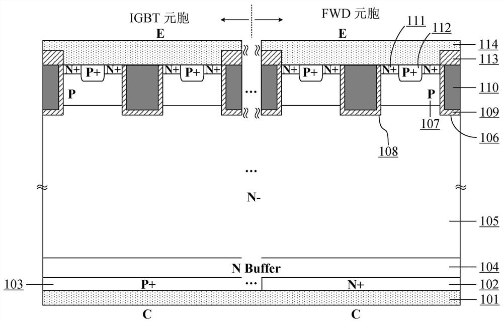
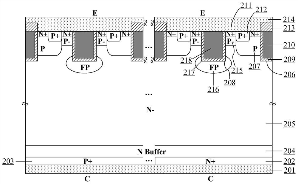
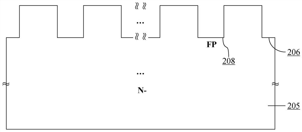
[0054] figure 2 It is a schematic cross-sectional view of an RC-IGBT device according to the first embodiment of the present invention. The device structure has: collector 201 at the bottom, heavily doped N above the collector 201 + Cathode region 202 and heavily doped P + The collector regions 203 are staggered, and the N-type buffer layer 204 is located in the heavily doped N + Cathode region 202 and heavily doped P + On the collector region 203, the N-type drift region 205 is located on the N-type buffer layer 204; the upper surface of the N-type drift region 205 is a plurality of repetitive front-side structures, and the minimum front-side structure unit includes: a trench gate structure 206, P-type base region 207, trench assisted gate structure 208, lightly doped P - P-type base region 215 and floating FP region 216; the trench gate structure 206 is sequentially filled with a first gate dielectric layer 209 and a first gate electrode 210, the P-type base region 207 ...

Embodiment 2

[0067] Figure 9 It is a schematic cross-sectional view of an RC-IGBT device according to the second embodiment of the present invention. compared to figure 2 The difference between the device structure in the first embodiment and the device structure in the second embodiment is that the upper surface of the floating FP region 316 is directly connected to the emitter electrode 314 at the bottom of the trench auxiliary gate structure 308, while figure 2 In the first embodiment, a Schottky contact is formed between the floating FP region 216 and the emitter electrode 214 . Second Embodiment This design increases the area of ​​the front-side emitter region of the RC-IGBT and the hole path, and the Schottky contact can control the hole injection efficiency, which is beneficial to reduce the on-voltage drop and reverse recovery loss of the device.

[0068] The device structure has a collector 301 at the bottom, heavily doped N above the collector 301 + Cathode region 302 and h...

Embodiment 3

[0080] Figure 18 It is a schematic cross-sectional view of the cell structure of the RC-IGBT device according to the third embodiment of the present invention. Compared with the device structure of the second embodiment of the present invention, the device structure of the third embodiment also has the following characteristics: the topography of the trench gate structure 406 and the trench auxiliary gate structure 408 is an inverted trapezoid, and lightly doped P - type base region 415 and its surface heavily doped with N + The type emitter regions 411 are located on the left and right sidewalls of the trench auxiliary gate structure 408 . This design increases the left and right sidewalls of the trench auxiliary gate structure as the front-side emitter area, which increases the conductive area, which is beneficial to improve the area ratio of the punch-through NPN triode structure on the front side, thereby enhancing the front-side FWD during freewheeling of the RC-IGBT. ...


PUM


Abstract

The invention discloses a power semiconductor device and a preparation method thereof, and belongs to the field of power semiconductor devices. A punch-through triode structure for extracting electrons in a drift region is introduced, so that the injection efficiency of a front hole is reduced, an emitter hole current is converted into an electron drift current, and the conduction voltage drop is not obviously increased; in addition, adjustment of punch-through area and position is realized by changing density and morphology of the front grooves, so that efficiency of electron extraction and front hole injection is changed, and design flexibility and design dimension of the device are improved.

Description

technical field [0001] The invention belongs to the field of power semiconductor devices, and relates to an insulated gate bipolar transistor (IGBT), in particular to a reverse conducting insulated gate bipolar transistor (RC-IGBT) device and a preparation method thereof. Background technique [0002] Reverse Conducting Insulated Gate Bipolar Transistor (RC-IGBT) device, due to the integration of Insulated Gate Bipolar Transistor (IGBT) and Freewheeling Diode (FWD) in the same cell, compared to discrete IGBT and FWD through For the integration of bonding wire packaging into a single device, it can bring advantages such as increased power density, reduced parasitic inductance, and increased chip area utilization, and is more widely used in power modules. With the above advantages of high integration, RC-IGBTs have been popularized in soft switching circuits, especially in induction heating applications. However, due to the limitation of switching frequency and switching loss,...

Claims


Application Information

Patent Timeline
Patent Type & Authority Applications(China)
IPC IPC(8): H01L29/739H01L29/06H01L21/331
CPCH01L29/7397H01L29/0619H01L29/66348Y02B70/10
Inventor 刘永冯浩单建安
Owner 安建科技(深圳)有限公司
Why Eureka
Try Eureka