Semiconductor light- emitting element, semiconductor light- emitting device, method for producing semiconductor light- emitting element, method for producing semiconductor light- emitting device, illumination device using semiconductor light-emitting device, and electronic apparatus

a light-emitting element and semiconductor technology, applied in semiconductor/solid-state device manufacturing, semiconductor devices, electrical devices, etc., can solve the problems of difficult extraction of light from the outside of the light-emitting layer through the portions of the transparent electrode where the bonding pads were formed, and achieve the effect of large light emission outpu

Active Publication Date: 2012-06-07
TOYODA GOSEI CO LTD
View PDF5 Cites 26 Cited by
  • Summary
  • Abstract
  • Description
  • Claims
  • Application Information

AI Technical Summary

Benefits of technology

[0027]The semiconductor light-emitting element according to the present invention is capable of suppressing, by forming the crystalline first transparent electrode layer and the non-crystalline second transparent electrode layer on the laminated semiconductor layer in which the n-type first semiconductor layer, the light-emitting layer...

Problems solved by technology

Since these bonding pads cut off light from the light-emitting layer, it was impossible to extract emitted light from the light-emitting layer through the portions on the transparent electrode where the bonding pads were formed.
Of these, the light traveling toward the substrate was ...

Method used


Image

  • Semiconductor light- emitting element, semiconductor light- emitting device, method for producing semiconductor light- emitting element, method for producing semiconductor light- emitting device, illumination device using semiconductor light-emitting device, and electronic apparatus
  • Semiconductor light- emitting element, semiconductor light- emitting device, method for producing semiconductor light- emitting element, method for producing semiconductor light- emitting device, illumination device using semiconductor light-emitting device, and electronic apparatus
  • Semiconductor light- emitting element, semiconductor light- emitting device, method for producing semiconductor light- emitting element, method for producing semiconductor light- emitting device, illumination device using semiconductor light-emitting device, and electronic apparatus

Examples


examples

[0208]Next, examples of the present invention will be described, but the present invention is not limited to the examples.

examples 1 to 5

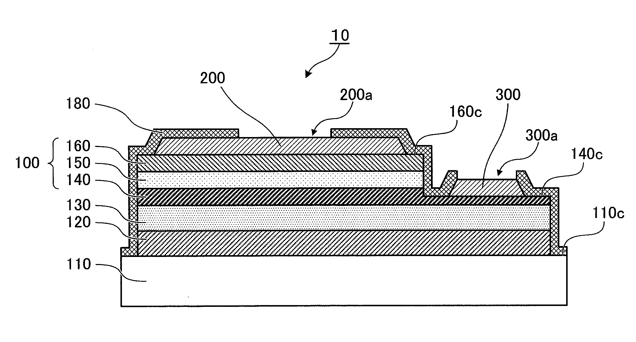
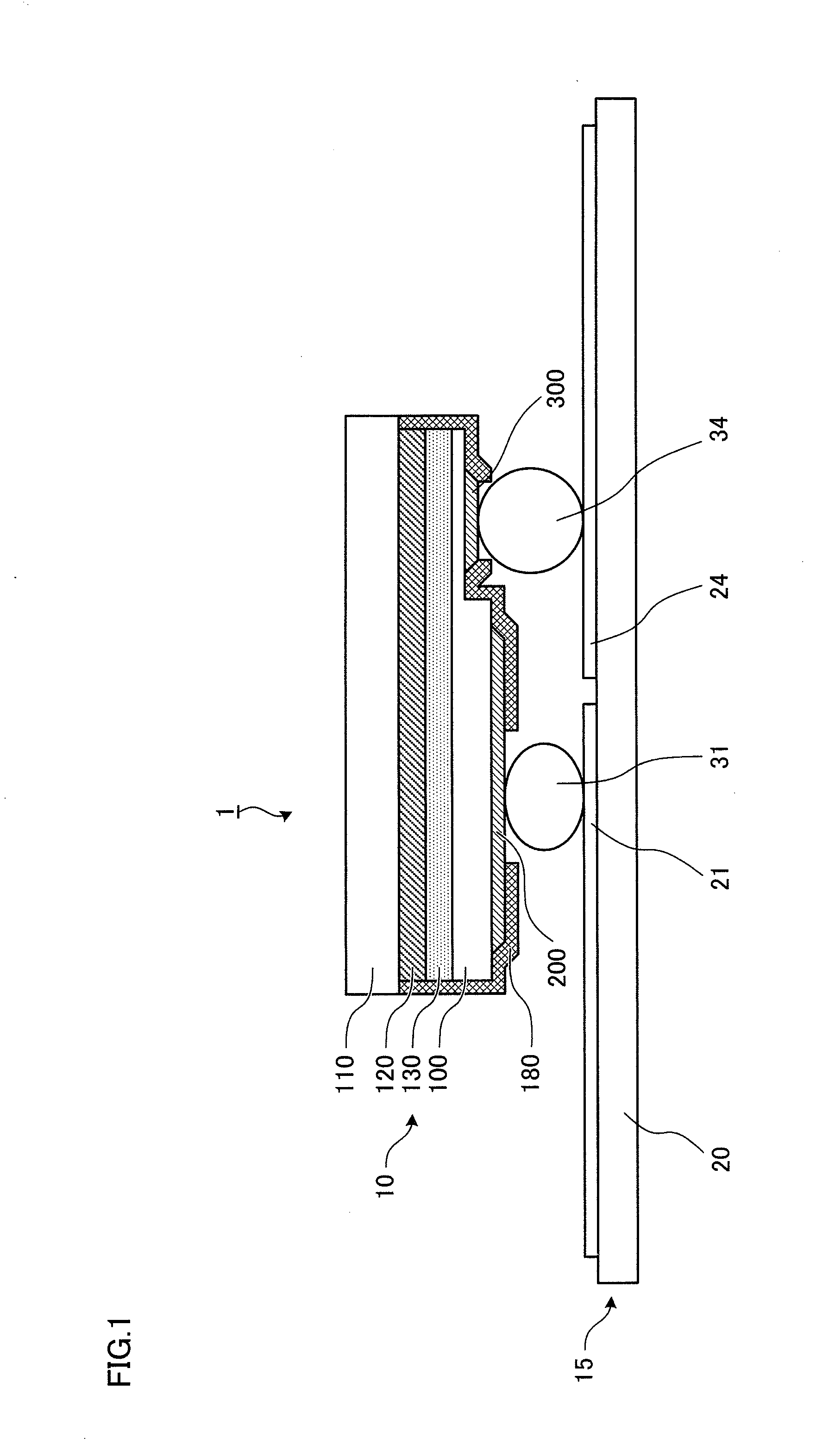
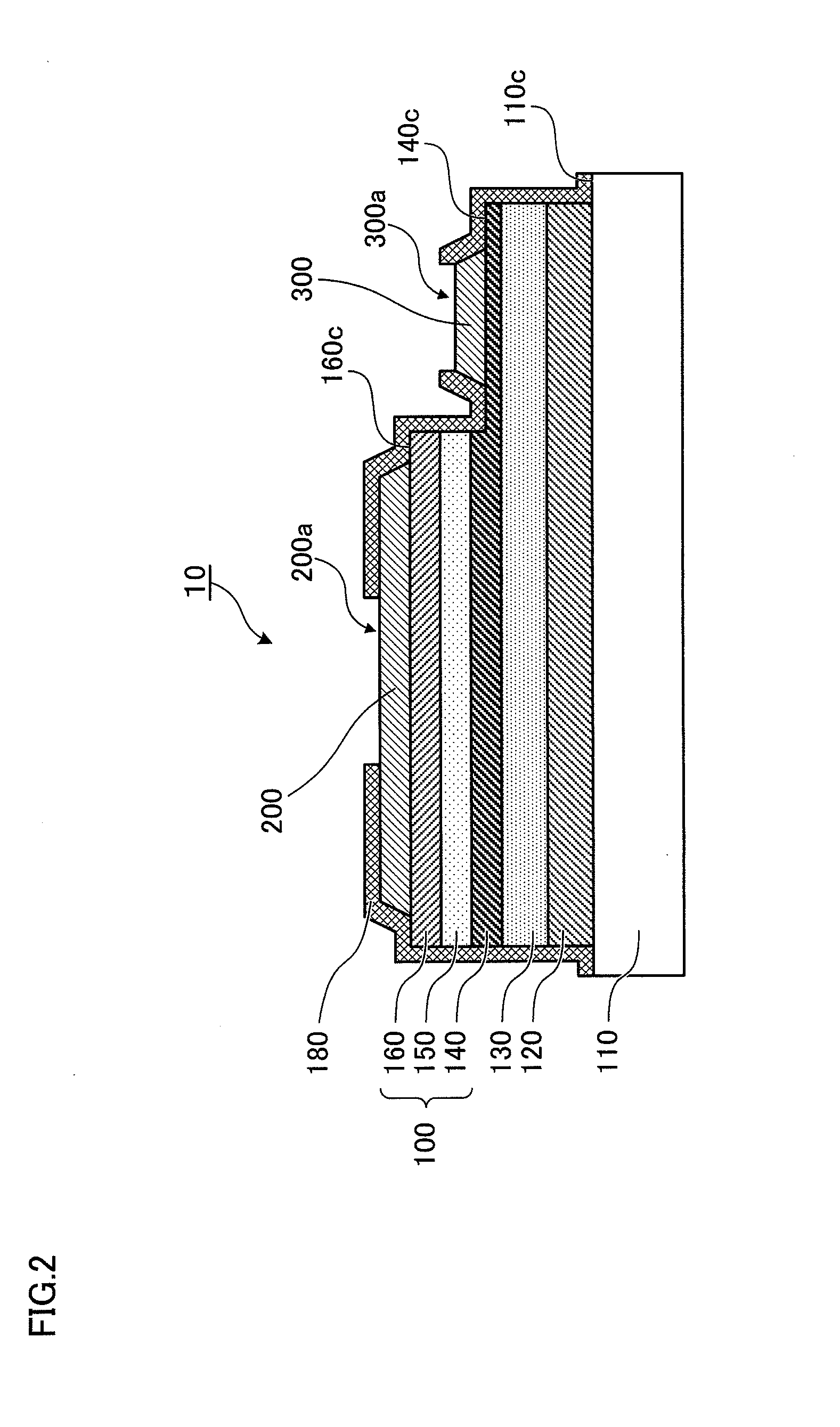
[0209]The semiconductor light-emitting element 10 used in Examples 1 to 5 has the same configuration as that shown in FIG. 2. The first electrode 200 has the same configuration as that shown in FIG. 5. The second electrode 300 has the same configuration as that shown in FIG. 6.

[0210]The substrate 110 is a sapphire substrate which is C-axis oriented. In Examples 1 to 5, the first transparent electrode layer 210 is the IZO film or the ITO film subjected to heat treatment. The thickness thereof differs in the examples 1 to 5. The second transparent electrode layer 220a is the amorphous IZO film with a thickness of 2 nm. The reflecting layer 220b is made of Ag, the first barrier layer 220c is made of Ta, the first bonding layer 230a is made of TaN, the second barrier layer 230b is made of Ta, the first metal layer 230c is made of Pt, the second metal layer 230d is made of Au and the second bonding layer 230e is made of Ta.


PUM


Abstract

The disclosed semiconductor light-emitting element is configured from layering an n-type semiconductor layer, a light-emitting layer, and a p-type semiconductor layer (160); and a first electrode (200), which is the cathode, is formed on the p-type semiconductor layer (160). Also, between the p-type semiconductor layer (160) and a reflecting layer (220b), the first electrode (200) is provided with a crystalline first transparent electrode layer (210) and a non-crystalline second transparent electrode layer (220a). The crystalline first transparent electrode layer (210) increases adhesion with the p-type semiconductor layer (160), and the non-crystalline second transparent electrode layer (220a) suppresses delamination of the reflecting layer (220b). Also, the first transparent electrode layer (210) and the second transparent electrode layer (220a) transmit light emitted from the light-emitting layer and suppress degradation of reflective characteristics. In this way, delamination of the reflecting layer and degradation of reflective characteristics are suppressed in a semiconductor light-emitting element mounted using flip-chip (FC) mounting.

Description

TECHNICAL FIELD[0001]The present invention relates to a semiconductor light-emitting element, a semiconductor light-emitting device, a method for producing the semiconductor light-emitting element, a method for producing the semiconductor light-emitting device, an illumination device using the semiconductor light-emitting device, and an electronic apparatus.BACKGROUND ART[0002]Recently, a GaN-based compound semiconductor has become a focus of attention as a semiconductor material of the light-emitting element of short wavelength light. The GaN-based compound semiconductor is formed by a metal organic chemical vapor deposition method (MOCVD method), a molecular beam epitaxy method (MBE method) or the like on a sapphire single crystal or other various oxides or group III-V compounds provided as a substrate.[0003]In a semiconductor light-emitting element using the GaN-based compound semiconductor, a laminated semiconductor layer having a light-emitting diode (LED) structure constituted...

Claims


Application Information

Patent Timeline
IPC IPC(8): H01L33/60H01L33/00
CPCH01L33/38H01L2224/13H01L33/42H01L33/405H01L2224/16225
Inventor OKABE, TAKEHIKOMASUYA, KYOUSUKE
Owner TOYODA GOSEI CO LTD
Why Eureka
Try Eureka